

TSV etching equipment focuses on creating channels with a high depth-to-width ratio inside silicon wafers. Today, the mainstream etching method uses dry etching technology, specifically reactive ion etching (RIE) or deep reactive ion etching (DRIE). These technologies achieve precise and efficient high-aspect-ratio etching of silicon wafers by exciting the formation of plasma on the surface of the silicon wafer and cleverly combining the dual effects of ion physical bombardment and chemical reaction.
According to our (Global Info Research) latest study, the global TSV Etching Equipment market size was valued at US$ 1101 million in 2024 and is forecast to a readjusted size of USD 1959 million by 2031 with a CAGR of 8.7% during review period.
Market segment by Type: 200mm Etching、 300mm Etching
Market segment by Application: Advanced Packaging、 MEMS、 Others
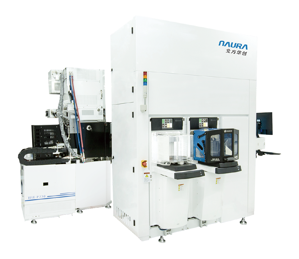
Major players covered: LAM、 KLA、 TEL、 Samco Inc、 GigaLane Co., Ltd、 AMEC、 NAURA、 ULVAC、 Jiangsu Alpha Semiconductor、 SPP Technologies Co., Ltd、 Shanghai Wintech、 Oxford Instruments
Market Drivers:
1. The continuous miniaturization of semiconductor devices, as defined by Moore’s Law and advanced packaging (e.g., 3D ICs), fundamentally drives demand for TSV etching equipment. Creating high-aspect-ratio, uniform vias for vertical interconnects requires highly precise and repeatable etching processes, making advanced etching tools indispensable for leading-edge logic, memory, and heterogeneous integration applications.
2. The explosive growth in data generation and artificial intelligence (AI) workloads necessitates higher-performance and higher-bandwidth memory solutions. This fuels the adoption of technologies like High Bandwidth Memory (HBM) and 3D NAND flash memory, both of which rely heavily on TSV etching for their stacked architectures, creating a sustained and growing equipment market.
3. The increasing complexity of device architectures and the introduction of new materials (such as novel etch-stop layers and dielectrics) require more sophisticated etching capabilities. This drives the need for next-generation TSV etchers with enhanced process control, selectivity, and the ability to handle diverse material stacks, pushing equipment manufacturers to innovate and upgrade their offerings.
Development Opportunities:
1. The rapid expansion of the HBM market, driven primarily by AI servers and accelerators, presents a significant near-term opportunity. Each new generation of HBM requires more TSV layers and greater etching precision, leading to increased demand for advanced etching equipment and potential for repeat sales as memory manufacturers scale production and migrate to newer designs.
2. The rise of heterogeneous integration and chiplet-based designs offers a substantial growth avenue. As the industry moves away from monolithic system-on-chips, there is growing need for TSV etching for silicon interposers, bridge chips, and through-silicon interposer (TSI) technologies, opening the equipment market to a broader range of applications beyond traditional memory.
3. Emerging applications in advanced sensors, MEMS, and photonics represent new frontiers. Technologies like image sensors for automotive LiDAR, advanced microphones, and silicon photonics for data communication increasingly utilize TSV for 3D integration and packaging, creating new, specialized niches for etching equipment tailored to these non-traditional semiconductor fields.
Market Restraining Factors:
1. The exceptionally high cost of advanced TSV etching equipment, often amounting to several million dollars per tool, poses a significant barrier to entry and expansion. This capital intensity can deter smaller players and foundries from rapid adoption, making purchasing cycles highly dependent on the capital expenditure (CapEx) cycles of large semiconductor manufacturers, which are often cyclical and volatile.
2. The complexity and technical challenges associated with etching very high-aspect-ratio TSVs with minimal bowing, scalloping, and sidewall damage create significant process development hurdles. Achieving the necessary uniformity, yield, and reliability across entire wafers, especially for larger wafer sizes like 300mm, can slow down technology adoption and increase the total cost of ownership for manufacturers.
- The emergence of competing interconnect and packaging technologies presents an alternative threat. While TSV is dominant for many 3D stacking applications, ongoing research and development into alternatives like hybrid bonding (which may reduce reliance on deep vias) or panel-level packaging could, in the longer term, potentially displace some demand for TSV-centric processes and the specialized equipment required for them.
Chapter 1, to describe TSV Etching Equipment product scope, market overview, market estimation caveats and base year.
Chapter 2, to profile the top manufacturers of TSV Etching Equipment, with price, sales quantity, revenue, and global market share of TSV Etching Equipment from 2021 to 2025.
Chapter 3, the TSV Etching Equipment competitive situation, sales quantity, revenue, and global market share of top manufacturers are analyzed emphatically by landscape contrast.
Chapter 4, the TSV Etching Equipment breakdown data are shown at the regional level, to show the sales quantity, consumption value, and growth by regions, from 2021 to 2032.
Chapter 5 and 6, to segment the sales by Type and by Application, with sales market share and growth rate by Type, by Application, from 2021 to 2032.
Chapter 7, 8, 9, 10 and 11, to break the sales data at the country level, with sales quantity, consumption value, and market share for key countries in the world, from 2021 to 2025.and TSV Etching Equipment market forecast, by regions, by Type, and by Application, with sales and revenue, from 2026 to 2032.
Chapter 12, market dynamics, drivers, restraints, trends, and Porters Five Forces analysis.
Chapter 13, the key raw materials and key suppliers, and industry chain of TSV Etching Equipment.
Chapter 14 and 15, to describe TSV Etching Equipment sales channel, distributors, customers, research findings and conclusion.
Global Info Research is a company that digs deep into global industry information to support enterprises with market strategies and in-depth market development analysis reports. We provides market information consulting services in the global region to support enterprise strategic planning and official information reporting, and focuses on customized research, management consulting, IPO consulting, industry chain research, database and top industry services. At the same time, Global Info Research is also a report publisher, a customer and an interest-based suppliers, and is trusted by more than 30,000 companies around the world. We will always carry out all aspects of our business with excellent expertise and experience.
About Us:
Global Info Research
Web: https://www.globalinforesearch.com
CN: 0086-176 6505 2062
HK: 00852-58030175
US: 001-347 966 1888
Email: report@globalinforesearch.com