

Semiconductor Optical Systems Market Summary
Semiconductor optical systems refer to high-precision optical components and systems used in semiconductor manufacturing, inspection, and optoelectronic device applications to precisely control, transmit, focus, or image light beams (typically ultraviolet or extreme ultraviolet lasers). Their core lies in utilizing high beam quality and adaptive technology to achieve micro- and nano-level precision in energy delivery and control during semiconductor manufacturing and inspection processes. Semiconductor manufacturing processes heavily rely on precision optical systems to achieve the required resolution, accuracy, and efficiency. This report primarily summarizes optical systems used in the semiconductor field.
According to the new market research report “Global Semiconductor Optical Systems Market Report 2026-2032”, published by QYResearch, the global Semiconductor Optical Systems market size is projected to reach USD 10.78 billion by 2032, at a CAGR of 8.5% during the forecast period.
Figure00001. Global Semiconductor Optical Systems Market Size (US$ Million), 2021-2032
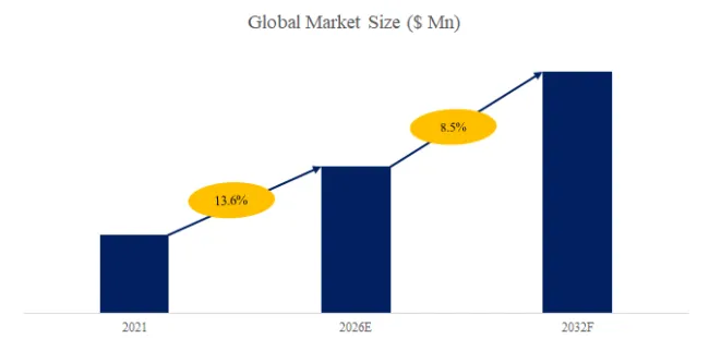
Above data is based on report from QYResearch: Global Semiconductor Optical Systems Market Report 2026-2032 (published in 2026). If you need the latest data, plaese contact QYResearch.
A Panoramic View of the Industry Chain: Collaborative Innovation, Building a Solid Industrial Foundation
The semiconductor optical system industry chain covers the entire ecosystem from basic materials to end applications. Upstream focuses on core materials and equipment, encompassing key raw materials such as high-purity silicon wafers, special photoresists, and optical-grade thin films, as well as precision manufacturing equipment such as lithography machines, etching machines, and ion implanters. Midstream centers on chip design and manufacturing, involving the development of digital circuits, analog circuits, and photonic integrated chips, relying on EDA tools to complete the entire process from architecture design to physical implementation. Downstream extends to diverse fields such as fiber optic communication, laser processing, medical imaging, and consumer electronics. For example, semiconductor lasers serve as a core light source in fiber optic communication, are used for precise surgical navigation in the medical field, and enable facial recognition and 3D sensing functions in consumer electronics. Close collaboration across all links of the industry chain ensures that upstream technological breakthroughs support midstream manufacturing, while downstream application demands drive the iterative upgrading of the industry chain.
Policy Empowerment: Strategic Guidance, Activating Industrial Innovation Momentum
National policies provide comprehensive support for the development of semiconductor optical systems. At the top-level design level, integrated circuits are listed as a key area for research and development under the new national system, with a clear goal of achieving self-sufficiency and control over high-end chips, key materials, and equipment during the 14th Five-Year Plan period. In terms of fiscal and tax incentives, a ten-year tax exemption policy will be implemented for integrated circuit manufacturing enterprises with a linewidth of less than 28nm, and tax incentives will be extended to the entire industry chain, including packaging, equipment, and materials, reducing enterprises’ R&D and production costs. Regarding the construction of the industrial ecosystem, the policy promotes deep integration of industry, academia, and research, supports universities in establishing integrated circuits as a first-level discipline, and cultivates interdisciplinary talents; it also encourages local governments to establish loan risk compensation mechanisms, guides commercial financial institutions to optimize financial services, and provides financial support for startups. Furthermore, the policy strengthens standard setting and intellectual property protection, accelerates the development of standards for third-generation semiconductor materials and devices, and aims to seize the technological high ground.
Trends and Opportunities: Technological Iteration, Opening Up Diverse Growth Tracks
Semiconductor optical systems are ushering in a dual opportunity of technological transformation and market expansion. On the technical front, in-memory computing architecture breaks through the bottlenecks of the “memory wall” and “power wall,” enabling in-situ data computation by embedding algorithms in memory, significantly improving AI computing efficiency. Data processing units (DPUs), as new infrastructure for data centers, offload virtualization, storage, and security tasks from the CPU, becoming the core carrier of intelligent computing power. Third-generation semiconductor materials (such as silicon carbide and gallium nitride), with their high efficiency and high power density, are accelerating the replacement of traditional silicon-based devices in new energy vehicles and photovoltaic inverters. On the market front, the explosive demand for AI computing power is driving growth in orders for advanced process chips, while the widespread adoption of 5G and the Internet of Things is generating massive demand for sensors. Emerging scenarios such as medical aesthetics and intelligent driving are opening up new markets for semiconductor lasers. For example, the application of silicon carbide power devices in the electric drive systems of new energy vehicles can reduce energy consumption and extend driving range, becoming a key area in the technological competition among automakers.
Challenges and Barriers: Breaking Bottlenecks and Forging Core Competitiveness
The obstacles to industry development are concentrated in three aspects: technology, capital, and ecosystem. Technologically, key components such as high-end lithography machines and EDA tools still rely on imports. Technical challenges such as the power of the EUV lithography light source and the loss of the reflectors have not yet been fully overcome, hindering breakthroughs in advanced processes. Cutting-edge technologies such as in-memory computing and quantum computing are still in the laboratory stage, and their commercialization paths are unclear. Financially, semiconductor optical systems have long development cycles and require large investments; a single EUV lithography machine costs over $200 million, making it difficult for small and medium-sized enterprises to afford the high equipment and tape-out costs. Ecosystem-wise, the efficiency of supply chain collaboration needs improvement. Issues such as inconsistent standards and difficulties in data interoperability exist in the design, manufacturing, and packaging stages, affecting overall innovation efficiency. Furthermore, international technology blockades and trade frictions increase supply chain risks, forcing companies to accelerate the process of domestic substitution.
The Path to Breakthrough: Collaborative Progress Towards the High End of the Global Value Chain
Faced with these challenges, the industry needs to be driven by innovation and build an open and collaborative industrial ecosystem. At the enterprise level, companies should focus on tackling key technologies in specific areas, integrating global resources through mergers and acquisitions and joint ventures to enhance core competitiveness; simultaneously, they should strengthen cooperation with universities and research institutions to promote deep integration of industry, academia, and research. At the policy level, it is necessary to improve the financial support system, guide social capital towards early-stage projects, and establish diversified financing channels; optimize talent policies to attract overseas high-end talent back to China and cultivate a local technological talent pool. At the industry chain level, it is essential to promote standardization across the upstream and downstream sectors, establish a data sharing platform, and improve collaborative efficiency; strengthen international cooperation, participate in global standard setting, and enhance China’s technological influence. Through multi-party collaboration, semiconductor optical systems will break through development bottlenecks and gain a proactive position in global industrial competition.
About The Authors
| Chengping Zhang | A experienced Technology & Market Analyst. Deep experience in chemical industry, focus on electronic materials, engineering materials and mineral resources, etc. Fully engaged in the development of technology and market reports as well as custom projects. | |
|
Senior Analyst |
||
| Email: zhangchengping@qyresearch.com |
Website: www.qyresearch.com Hot Line:4006068865
QYResearch focus on Market Survey and Research
US: +1-888-365-4458(US) +1-202-499-1434(Int’L)
EU: +44-808-111-0143(UK) +44-203-734-8135(EU)
Asia: +86-10-8294-5717(CN) +852-30628839(HK)
About QYResearch
QYResearch founded in California, USA in 2007.It is a leading global market research and consulting company. With over 17 years’ experience and professional research team in various cities over the world QY Research focuses on management consulting, database and seminar services, IPO consulting (data is widely cited in prospectuses, annual reports and presentations), industry chain research and customized research to help our clients in providing non-linear revenue model and make them successful. We are globally recognized for our expansive portfolio of services, good corporate citizenship, and our strong commitment to sustainability. Up to now, we have cooperated with more than 60,000 clients across five continents. Let’s work closely with you and build a bold and better future.
QYResearch is a world-renowned large-scale consulting company. The industry covers various high-tech industry chain market segments, spanning the semiconductor industry chain (semiconductor equipment and parts, semiconductor materials, ICs, Foundry, packaging and testing, discrete devices, sensors, optoelectronic devices), photovoltaic industry chain (equipment, cells, modules, auxiliary material brackets, inverters, power station terminals), new energy automobile industry chain (batteries and materials, auto parts, batteries, motors, electronic control, automotive semiconductors, etc.), communication industry chain (communication system equipment, terminal equipment, electronic components, RF front-end, optical modules, 4G/5G/6G, broadband, IoT, digital economy, AI), advanced materials industry Chain (metal materials, polymer materials, ceramic materials, nano materials, etc.), machinery manufacturing industry chain (CNC machine tools, construction machinery, electrical machinery, 3C automation, industrial robots, lasers, industrial control, drones), food, beverages and pharmaceuticals, medical equipment, agriculture, etc.
About Us:
QYResearch founded in California, USA in 2007, which is a leading global market research and consulting company. Our primary business include market research reports, custom reports, commissioned research, IPO consultancy, business plans, etc. With over 18 years of experience and a dedicated research team, we are well placed to provide useful information and data for your business, and we have established offices in 7 countries (include United States, Germany, Switzerland, Japan, Korea, China and India) and business partners in over 30 countries. We have provided industrial information services to more than 60,000 companies in over the world.
Contact Us:
If you have any queries regarding this report or if you would like further information, please contact us:
QY Research Inc.
Add: 17890 Castleton Street Suite 369 City of Industry CA 91748 United States
EN: https://www.qyresearch.com
Email: global@qyresearch.com
Tel: 001-626-842-1666(US)
JP: https://www.qyresearch.co.jp


