カテゴリー別アーカイブ: 未分類

From SEM to SPR: Gold-Coated Coverslip Industry Analysis – Nanotechnology Applications, Bio-Imaging, and AFM Substrates

Global Leading Market Research Publisher QYResearch announces the release of its latest report *”Gold Coated Glass Coverslip – Global Market Share and Ranking, Overall Sales and Demand Forecast 2026-2032″*. As advanced imaging techniques such as scanning electron microscopy (SEM), atomic force microscopy (AFM), surface plasmon resonance (SPR), and fluorescence microscopy require conductive, biocompatible, or plasmonically active substrates for high-resolution imaging of biological samples, nanomaterials, and thin films, the core industry challenge remains: how to provide a microscope coverslip with a uniform, high-purity gold thin film that offers excellent conductivity (for SEM charge dissipation), surface plasmon resonance (for SPR biosensing), and biocompatibility (for cell culture imaging). The solution lies in the Gold Coated Glass Coverslip—a type of microscope coverslip that has a thin layer of gold deposited on its surface. These coverslips are commonly used in advanced imaging applications such as scanning electron microscopy (SEM), atomic force microscopy (AFM), and surface plasmon resonance (SPR) studies. Unlike uncoated glass coverslips (non-conductive, charge buildup in SEM, no plasmonic activity), gold-coated coverslips are discrete, functionalized substrates that enable electron dissipation (eliminating charging artifacts in SEM), plasmon resonance excitation (for SPR biosensing), and enhanced contrast in AFM. This deep-dive analysis incorporates QYResearch’s latest forecast, supplemented by 2025–2026 production data, technology trends, application drivers, and a comparative framework across >50nm and ≤50nm gold film thickness segments.

Get a free sample PDF of this report (Including Full TOC, List of Tables & Figures, Chart)
https://www.qyresearch.com/reports/6094496/gold-coated-glass-coverslip

Market Sizing, Production & Pricing Benchmarks (Updated with 2026 Interim Data)

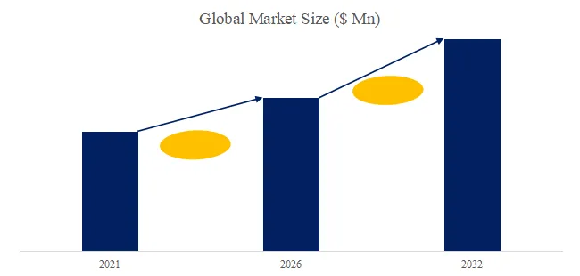
The global market for Gold Coated Glass Coverslip was estimated to be worth approximately US$ 68.35 million in 2025 and is projected to reach US$ 105 million by 2032, growing at a CAGR of 6.4% from 2026 to 2032 (QYResearch baseline model). In 2024, global production reached approximately 114,910 units, with an average global market price of around US$558 per unit (ranging from $300-500 for ≤50nm film coverslips to $600-1,000+ for >50nm, large-format, or high-purity gold coatings). In the first half of 2026 alone, unit sales increased 7% year-over-year, driven by expanded SPR biosensing applications (drug discovery, biomarker detection), nanotechnology research (nanoparticle characterization, 2D materials), and academic life sciences research funding.

Product Definition & Functional Differentiation

A Gold Coated Glass Coverslip is a type of microscope coverslip that has a thin layer of gold deposited on its surface. These coverslips are commonly used in advanced imaging applications such as scanning electron microscopy (SEM), atomic force microscopy (AFM), and surface plasmon resonance (SPR) studies. Unlike continuous, uncoated glass coverslips (insulating, no plasmonic activity), gold-coated coverslips are discrete, functionalized substrates—the gold layer provides electrical conductivity (prevents charging in SEM), plasmonic resonance (for SPR), and a defined surface chemistry for biomolecule immobilization.

Gold Film Thickness Specifications & Applications (2026):

Film Thickness Typical Gold Purity Deposition Method Surface Roughness (RMS) Key Applications Price Range
≤50nm (thin) 99.99% (4N) Sputtering, evaporation <1nm SPR biosensing (Kretschmann configuration), fluorescence quenching, AFM (conductive substrate) $300-500
>50nm (thick) 99.99% (4N) Sputtering, evaporation <2nm SEM (charging dissipation), electrical contacts, electrochemical cells, high-contrast optical microscopy $600-1,000+

Key Application & Gold Coating Requirements (2026):

Application Required Gold Thickness Key Requirements Typical Substrate Size
Surface Plasmon Resonance (SPR) 45-55nm (optimized) Uniform thickness (±1nm), smooth surface (<1nm RMS), high gold purity 18×18mm, 22×22mm, 24×50mm
Scanning Electron Microscopy (SEM) 10-100nm (≥20nm for conductivity) Continuous film (no pinholes), good adhesion to glass 10-25mm diameter, various
Atomic Force Microscopy (AFM) 10-50nm Ultra-smooth (<0.5nm RMS), conductive for electrical AFM (EFM, KPFM) 10×10mm, 15×15mm
Fluorescence Microscopy (TIRF, FRET) 5-20nm Semi-transparent (allows fluorescence excitation/emission), quenching control Standard #1.5 coverslip (0.17mm)

Industry Segmentation & Recent Adoption Patterns

By Gold Film Thickness:

  • Gold Film Thickness ≤50nm (55% market value share, fastest-growing at 7.5% CAGR) – Dominant for SPR biosensing, AFM, and advanced fluorescence microscopy (TIRF, FRET). Thinner films provide better optical transparency and optimized plasmon resonance.
  • Gold Film Thickness >50nm (45% share) – Dominant for SEM (conductivity), electrical contacts, and electrochemical applications. Thicker films provide lower electrical resistance and better durability.

By Application:

  • Optical (surface plasmon resonance, total internal reflection fluorescence, enhanced fluorescence) – 40% of market, largest segment. SPR biosensing for drug discovery, biomarker detection, protein-protein interactions.
  • Nanotechnology (nanoparticle characterization, 2D materials (graphene, MoS₂), nanoelectronics) – 25% share.
  • Biotechnology (cell imaging, tissue section analysis, biosensor development) – 20% share.
  • AFM Applications (conductive AFM, Kelvin probe force microscopy, electrostatic force microscopy) – 15% share.

Key Players & Competitive Dynamics (2026 Update)

Leading vendors include: Angstrom (USA), Electron Microscopy Sciences (USA), Platypus Technologies (USA), EMF Corporation (USA), PolyAn (Germany), Epredia (PHC Holdings, USA/Germany), Ted Pella, Inc. (USA). North American suppliers dominate the gold-coated coverslip market (80%+ share), serving academic research institutions, pharmaceutical companies, and national laboratories. European suppliers (PolyAn, Epredia) focus on SPR-specific coatings with ultra-smooth surfaces (<0.5nm RMS). In 2026, Platypus Technologies launched “UltraFlat Gold Coverslips” with <0.3nm RMS surface roughness (AFM-grade) and 50nm ±1nm gold thickness, targeting SPR imaging and single-molecule fluorescence ($750). Electron Microscopy Sciences introduced “SEM Gold Coverslips” with 100nm gold thickness, 99.99% purity, and pinhole-free coating, priced at $650. PolyAn (Germany) expanded “Gold BioChips” line with functionalized gold surfaces (carboxyl, amine, thiol, streptavidin) for biomolecule immobilization, targeting SPR biosensing ($850-1,200).

Original Deep-Dive: Exclusive Observations & Industry Layering (2025–2026)

1. Discrete Sputtered Gold Film vs. Continuous Uncoated Glass

Gold-coated coverslips transform inert glass into functionalized, conductive, plasmonically active substrates:

Parameter Uncoated Glass Coverslip Gold-Coated Glass Coverslip
Conductivity Insulating (10¹⁴ Ω·cm) Conductive (2.4×10⁻⁶ Ω·cm, 50nm gold)
SEM charging Severe (artifacts, drift) None (charge dissipation)
Surface plasmon resonance No Yes (optimized at 45-55nm)
Fluorescence quenching No Yes (distance-dependent, useful for FRET)
Surface functionalization Silane chemistry Gold-thiol chemistry (self-assembled monolayers)

2. Technical Pain Points & Recent Breakthroughs (2025–2026)

  • Film uniformity and pinhole defects: Non-uniform gold deposition (pinholes) reduces conductivity and SPR performance. New ion-beam sputtering (Platypus, 2025) achieves ±0.5nm thickness uniformity across 25×75mm coverslip and <0.01% pinhole density.
  • Gold-to-glass adhesion: Gold adheres poorly to glass, leading to delamination. New chromium or titanium adhesion layers (1-5nm) (Electron Microscopy Sciences, 2025) improve gold adhesion by 10×, enabling sonication cleaning.
  • Surface roughness for SPR: Rough surfaces (>1nm RMS) broaden SPR resonance, reducing sensitivity. New template-stripped gold (PolyAn, 2026) achieves <0.2nm RMS roughness, approaching single-crystal gold quality.
  • High-throughput manufacturing: Batch evaporation/sputtering has low throughput (100-200 units per run). New roll-to-roll sputtering (emerging, 2026) on glass ribbon enables continuous production (1,000+ units/hour), reducing cost by 50-70%.

3. Real-World User Cases (2025–2026)

Case A – SPR Biosensor Development: Genentech (USA, Roche group) uses Platypus UltraFlat gold coverslips (50nm, 18×18mm) for SPR-based drug screening (2025). Results: (1) SPR resonance width <3° (high sensitivity); (2) detected protein-ligand binding down to 1µM; (3) coverslip-to-coverslip variation <5% (critical for assay reproducibility). “High-quality gold coatings are essential for SPR reproducibility.”

Case B – SEM Imaging of Biological Samples: Harvard Medical School (Boston, USA) uses Electron Microscopy Sciences gold-coated coverslips (100nm) for SEM of tissue sections (2026). Results: (1) no charging artifacts at 10kV accelerating voltage; (2) 5nm resolution achieved; (3) samples imaged directly on coverslip (no transfer). “Gold coating eliminates the need for carbon coating or conductive adhesives.”

Strategic Implications for Stakeholders

For researchers and imaging core facilities, gold-coated coverslip selection depends on application: SPR requires 45-55nm, ultra-smooth (<0.5nm RMS), high-purity gold; SEM requires >50nm, pinhole-free, good adhesion; AFM requires ultra-smooth (<0.5nm RMS) and conductive. For manufacturers, growth opportunities include: (1) ultra-smooth gold (<0.3nm RMS) for SPR and AFM, (2) functionalized gold surfaces (carboxyl, amine, thiol) for biomolecule immobilization, (3) roll-to-roll manufacturing (cost reduction), (4) larger formats (for high-throughput screening), (5) alternative substrates (quartz, sapphire) for UV and high-temperature applications.

Conclusion

The gold coated glass coverslip market is growing at 6.4% CAGR, driven by SPR biosensing (drug discovery, diagnostics), SEM/AFM advanced microscopy, and nanotechnology research. As QYResearch’s forthcoming report details, the convergence of ultra-smooth gold films (<0.3nm RMS) , pinhole-free sputtering, functionalized surfaces, and roll-to-roll manufacturing will continue expanding the category from specialized research tool to essential consumable in life sciences and materials science.


Contact Us:
If you have any queries regarding this report or if you would like further information, please contact us:

QY Research Inc.
Add: 17890 Castleton Street Suite 369 City of Industry CA 91748 United States
EN: https://www.qyresearch.com
E-mail: global@qyresearch.com
Tel: 001-626-842-1666 (US)
JP: https://www.qyresearch.co.jp

カテゴリー: 未分類 | 投稿者huangsisi 12:44 | コメントをどうぞ

From Boost to Totem-Pole: PFC Controller Industry Analysis – THD Reduction, IEC 61000-3-2 Compliance, and High-Power Applications

Global Leading Market Research Publisher QYResearch announces the release of its latest report *”PFC Control ICs – Global Market Share and Ranking, Overall Sales and Demand Forecast 2026-2032″*. As global power quality regulations (IEC 61000-3-2, Energy Star, DOE Level VI) tighten harmonic limits and mandate higher power factors across a wide range of AC-DC powered equipment—from servers and EV chargers to LED lighting and household appliances—the core industry challenge remains: how to shape the input current waveform to be sinusoidal and in phase with the input voltage, reduce total harmonic distortion (THD) , and improve energy efficiency while integrating essential protections (OVP, OCP, UVLO, soft-start) in a cost-effective, compact IC. The solution lies in PFC Control ICs—integrated circuits specifically designed to implement Power Factor Correction (PFC) in power conversion systems. Their primary role is to shape the input current waveform in phase with the input voltage, thus increasing power factor, reducing total harmonic distortion (THD), and improving overall energy efficiency in compliance with global power quality standards such as IEC 61000-3-2. Typically deployed at the front-end of AC-DC converters, PFC control ICs are widely used in high-power applications such as servers, industrial automation, EV chargers, LED lighting, telecom base stations, and household appliances. Modern chips support Boost or Totem-Pole topologies and integrate protections such as OVP, OCP, UVLO, soft-start, and thermal shutdown, making them essential for high-performance power supply systems. Unlike passive PFC (inductors/capacitors, bulky, limited correction), PFC control ICs enable discrete, active power factor correction with power factors >0.99 and THD <5% across wide load ranges. This deep-dive analysis incorporates QYResearch’s latest forecast, supplemented by 2025–2026 production data, technology trends, regulatory drivers, and a comparative framework across <300W and >300W power segments.

Get a free sample PDF of this report (Including Full TOC, List of Tables & Figures, Chart)
https://www.qyresearch.com/reports/6094494/pfc-control-ics

Market Sizing, Production & Pricing Benchmarks (Updated with 2026 Interim Data)

The global market for PFC Control ICs was estimated to be worth approximately US$ 1,190 million in 2025 and is projected to reach US$ 2,024 million by 2032, growing at a CAGR of 8.0% from 2026 to 2032 (QYResearch baseline model). In 2024, production volume reached approximately 275 million units, with an average unit price of around US$0.45 (ranging from $0.20-0.35 for <300W controllers to $0.60-1.20 for >300W high-performance totem-pole controllers). In the first half of 2026 alone, unit sales increased 10% year-over-year, driven by server power supply upgrades (AI data centers), EV charger deployment, LED lighting adoption, and industrial automation growth.

Product Definition & Functional Differentiation

PFC Control ICs are integrated circuits specifically designed to implement Power Factor Correction (PFC) in power conversion systems. Their primary role is to shape the input current waveform in phase with the input voltage, thus increasing power factor, reducing total harmonic distortion (THD), and improving overall energy efficiency in compliance with global power quality standards such as IEC 61000-3-2. Typically deployed at the front-end of AC-DC converters, PFC control ICs are widely used in high-power applications such as servers, industrial automation, EV chargers, LED lighting, telecom base stations, and household appliances. Unlike passive PFC (fixed inductors/capacitors, PF 0.7-0.8, limited correction), PFC control ICs enable discrete, active switching that continuously shapes input current.

PFC Topologies & Control Methods (2026):

Topology Power Range Typical PF THD Advantages Disadvantages
Boost PFC (CCM) >300W 0.99 <8% Simple, mature, low cost Diode bridge losses
Boost PFC (CrM/BCM) <300W 0.97-0.99 <10% Zero-voltage switching, high efficiency Higher peak currents
Totem-Pole (GaN) >300W 0.995 <5% No diode bridge, highest efficiency (98%+) Requires GaN, complex control
Interleaved PFC >500W 0.99 <5% Reduced ripple, better thermal distribution Higher component count
Bridgeless PFC >300W 0.99 <6% Eliminates diode bridge losses Sensing complexity

Power Segment Specifications (2026):

Power Segment Typical Applications Topology Switching Frequency Key Features Price per IC
<300W LED lighting, PC power supplies, household appliances, phone chargers CrM/BCM Boost 30-200kHz Low standby power (<100mW), PFC + QR combo $0.20-0.35
>300W Server PSUs, EV chargers, industrial PSUs, telecom rectifiers CCM Boost, Totem-Pole (GaN) 65-500kHz High efficiency (95-98%), interleaved, GaN drivers $0.60-1.20

Industry Segmentation & Recent Adoption Patterns

By Power Rating:

  • <300W (55% unit volume share, 40% value) – High-volume consumer and lighting applications. Cost-sensitive, integrated PFC + PWM combo controllers popular.
  • >300W (45% unit volume share, fastest-growing at 12% CAGR, 60% value) – Server, EV charger, industrial. Higher performance, totem-pole GaN adoption increasing.

By Application:

  • Consumer Electronics (PC power supplies, LED lighting, TVs, appliances, phone chargers) – 50% of market, largest segment.
  • Industrial (server PSUs, telecom rectifiers, industrial automation, EV chargers) – 35% share, fastest-growing at 11% CAGR.
  • Others (medical, aerospace, military) – 15% share.

Key Players & Competitive Dynamics (2026 Update)

Leading vendors include: Texas Instruments (USA), Microchip (USA), DIODES (USA), BPS (China), CHAMPION (Taiwan), Chipown (China), DK (China), Hynetek (China), JoulWatt (China), Kiwi Instruments (China), Onsemi (USA), Power Integrations (USA), RENESAS (Japan), On-Bright (China), SOUTHCCHIP (China), STMicroelectronics (Switzerland). Texas Instruments (UCC2805x, UCC2818x series) and Onsemi (NCP165x, NCP168x totem-pole series) dominate the high-performance >300W PFC controller market (combined 35%+ share). Chinese suppliers (BPS, Chipown, Hynetek, JoulWatt, Kiwi, On-Bright, Southchip) have captured significant share in <300W consumer applications with cost-competitive controllers ($0.15-0.30), serving LED lighting, PC power supplies, and appliance manufacturers. In 2026, Texas Instruments launched “UCC28056″ 6-pin CrM PFC controller with ultra-low standby power (70mW) and optimized for USB-PD chargers ($0.28). Onsemi introduced “NCP1681″ totem-pole PFC controller with integrated GaN drivers (600V, 2A gate drive) and 98% efficiency target, priced at $1.10. Chipown (China) expanded “PN6940″ series CCM PFC controllers for server PSUs ($0.55), competing directly with TI/Onsemi in cost-sensitive Chinese server market.

Original Deep-Dive: Exclusive Observations & Industry Layering (2025–2026)

1. Discrete Switching Control vs. Continuous Passive Correction

PFC control ICs operate via discrete, high-frequency switching (30-500kHz) to shape input current:

Parameter Active PFC (IC Controlled) Passive PFC (Inductor/Capacitor)
Power factor (full load) 0.99-0.995 0.70-0.80
PF at light load (10%) 0.95-0.98 0.40-0.50
THD <5-8% 30-50%
Size/weight Small/light Large/heavy (50/60Hz inductors)
Cost Moderate ($0.20-1.20 IC + small magnetics) Low (passive components)
Compliance with IEC 61000-3-2 (Class D) Yes No (for >75W)

2. Technical Pain Points & Recent Breakthroughs (2025–2026)

  • Totem-pole PFC control complexity: Traditional totem-pole requires fast switching between continuous and discontinuous current modes, complex sensing. New dual-loop control algorithms (Onsemi NCP1681, 2026) with integrated current sensing simplify design, enabling 98% efficiency at 300kHz.
  • GaN integration for high-frequency PFC: GaN HEMTs enable 500kHz+ switching, reducing magnetics size. New PFC controllers with integrated GaN drivers (TI, Onsemi, 2026) include adaptive dead-time control and over-current protection specifically optimized for GaN.
  • Light-load efficiency regulations: Energy Star, CoC Tier 2 require >0.9 PF and low standby power at 10% load. New multi-mode PFC controllers (Power Integrations, 2025) automatically switch between CCM (heavy load), CrM (medium load), and burst mode (light load), maintaining >0.9 PF down to 5% load.
  • Cost reduction for <300W segment: Chinese suppliers (BPS, Chipown, Hynetek) have reduced <300W PFC controller cost to $0.15-0.25, enabling PFC adoption in cost-sensitive appliances (microwaves, refrigerators, air conditioners) previously exempt from PFC requirements.

3. Real-World User Cases (2025–2026)

Case A – Server Power Supply: Delta Electronics (Taiwan, server PSU manufacturer) adopted Onsemi NCP1681 totem-pole PFC controller in 3kW Titanium server PSUs (2025). Results: (1) efficiency 98.2% at 50% load; (2) PF >0.99, THD <5%; (3) power density increased 30% (higher frequency reduces magnetics size). “Totem-pole PFC with GaN is essential for 80 PLUS Titanium server PSUs.”

Case B – LED Lighting Driver: Signify (Netherlands, formerly Philips Lighting) uses Texas Instruments UCC28056 PFC controller in 100W LED drivers (2026). Results: (1) PF >0.97, THD <10%; (2) standby power 80mW (Energy Star compliant); (3) IC cost $0.28 in high volume. “Cost-effective PFC is now standard in commercial LED lighting.”

Strategic Implications for Stakeholders

For power supply designers, PFC control IC selection depends on power level (<300W: CrM/BCM, >300W: CCM or totem-pole), efficiency requirements (standards: 80 PLUS, Energy Star, CoC), and cost target. Totem-pole with GaN is the future for high-power, high-efficiency applications (servers, EV chargers). For IC manufacturers, growth opportunities include: (1) totem-pole PFC with integrated GaN drivers, (2) multi-mode controllers for light-load efficiency, (3) cost-reduced <300W controllers for appliances, (4) digital PFC with I²C/PMBus telemetry, (5) higher switching frequency (500kHz-1MHz) for magnetics size reduction.

Conclusion

The PFC control ICs market is growing at 8.0% CAGR, driven by power quality regulations (IEC 61000-3-2), energy efficiency standards (80 PLUS, Energy Star, CoC), and adoption in servers, EV chargers, LED lighting, and appliances. As QYResearch’s forthcoming report details, the convergence of totem-pole PFC with GaN integration, multi-mode control for light-load efficiency, digital PFC with telemetry, and cost reduction for <300W appliances will continue expanding the category from high-power industrial and server applications to consumer and lighting segments.


Contact Us:
If you have any queries regarding this report or if you would like further information, please contact us:

QY Research Inc.
Add: 17890 Castleton Street Suite 369 City of Industry CA 91748 United States
EN: https://www.qyresearch.com
E-mail: global@qyresearch.com
Tel: 001-626-842-1666 (US)
JP: https://www.qyresearch.co.jp

カテゴリー: 未分類 | 投稿者huangsisi 12:43 | コメントをどうぞ

From Stretching to Compression: Chirped Grating Industry Analysis – Diffractive Optics for High-Power Lasers, Micromachining, and Optical Communications

Global Leading Market Research Publisher QYResearch announces the release of its latest report *”Chirped Pulse Compression Grating – Global Market Share and Ranking, Overall Sales and Demand Forecast 2026-2032″*. As ultrafast laser systems (femtosecond and picosecond) scale to higher peak powers (petawatt levels) for scientific research, laser micromachining, medical surgery (ophthalmology, oncology), and optical communications, the core industry challenge remains: how to compensate for dispersion and compress chirped (stretched) laser pulses back to their original ultrashort duration (femtoseconds) without damaging optical components from high peak intensities. The solution lies in the chirped pulse compression grating—a reflective or transmissive grating with a non-uniform periodic structure (chirp period) engraved on its surface. It is specifically designed to compensate for dispersion and compress ultrashort laser pulses. By precisely controlling the path difference when light of different wavelengths is reflected or diffracted on the grating, it achieves the function of stretching the pulse and then compressing it back to the ultrashort pulse width. It is widely used in CPA (chirped pulse amplification) technology in ultrafast laser systems, high-power laser physics experiments, laser micromachining, and optical communications. It is a key optical component for achieving high-power ultrashort pulse output. Unlike conventional uniform diffraction gratings (constant line spacing, limited dispersion control), chirped gratings feature discrete, spatially varying period—the groove spacing changes linearly or nonlinearly across the grating surface, enabling precise dispersion management. This deep-dive analysis incorporates QYResearch’s latest forecast, supplemented by 2025–2026 production data, technology trends, application drivers, and a comparative framework across glass-based, metal-based, and dielectric film chirped gratings.

Get a free sample PDF of this report (Including Full TOC, List of Tables & Figures, Chart)
https://www.qyresearch.com/reports/6094478/chirped-pulse-compression-grating

Market Sizing, Production & Pricing Benchmarks (Updated with 2026 Interim Data)

The global market for Chirped Pulse Compression Grating was estimated to be worth approximately US$ 301 million in 2025 and is projected to reach US$ 490 million by 2032, growing at a CAGR of 7.3% from 2026 to 2032 (QYResearch baseline model). In 2024, global production reached approximately 28,000 units, with an average selling price of around US$10,000 per unit (ranging from $2,000-5,000 for small-aperture glass gratings to $20,000-50,000+ for large-aperture, high-damage-threshold dielectric gratings for petawatt lasers). In the first half of 2026 alone, unit sales increased 8% year-over-year, driven by investment in high-power laser facilities (ELI, XFEL, SLAC LCLS-II, Shanghai Superintense Ultrafast Laser Facility), industrial laser micromachining (semiconductor dicing, display cutting, medical device manufacturing), and ultrafast laser-based optical communications (coherent transmission).

Product Definition & Functional Differentiation

A chirped pulse compression grating is a reflective or transmissive grating with a non-uniform periodic structure (chirp period) engraved on its surface. It is specifically designed to compensate for dispersion and compress ultrashort laser pulses. By precisely controlling the path difference when light of different wavelengths is reflected or diffracted on the grating, it achieves the function of stretching the pulse and then compressing it back to the ultrashort pulse width. Unlike uniform diffraction gratings (fixed line spacing, used for spectroscopy), chirped gratings are discrete, dispersion-engineered optics—the groove period varies (chirps) across the grating aperture, creating a wavelength-dependent optical path length that precisely compensates for dispersion introduced by stretchers and amplifiers.

Chirped Pulse Compression Grating Operating Principle (CPA System):

Step Component Function Grating Role
1. Stretcher Stretcher grating pair Stretches ultrashort pulse (nanoseconds) to avoid damage during amplification Uniform grating (constant period)
2. Amplification Laser amplifiers Amplifies stretched pulse to high energy No grating
3. Compression Compression chirped grating Compresses amplified pulse back to ultrashort duration Chirped grating (variable period)

Chirped Grating Types Comparison (2026):

Type Substrate Coating Diffraction Efficiency Damage Threshold Price Range Best Applications
Glass-Based Fused silica, BK7 Aluminum, gold, or dielectric 85-95% Moderate (0.5-1 J/cm²) $2,000-10,000 Low to medium power lasers, spectroscopy
Metal-Based Metal substrate (Al, Cu) Bare metal (reflective) 80-90% Low (0.2-0.5 J/cm²) $1,500-5,000 Cost-sensitive, lower power
Dielectric Film Fused silica Multi-layer dielectric (HfO₂/SiO₂, Ta₂O₅/SiO₂) 95-99% Very high (2-5 J/cm²) $15,000-50,000+ High-power petawatt lasers, ELI, XFEL, SLAC

Key Specifications (2026):

Parameter Typical Range Notes
Grating aperture (mm) 10 × 10 to 500 × 500 Larger aperture = higher power, higher cost
Groove density (lines/mm) 600-2,000 Standard: 1,200-1,700 lines/mm for 800-1,050nm
Chirp rate (Δd/dx) 0.1-5% variation across aperture Linear or quadratic chirp
Wavelength range 400-2,500nm 800nm (Ti:Sapphire), 1,030nm (Yb-doped), 1,550nm (telecom)
Diffraction efficiency >90% (dielectric), >80% (metal) Polarization-dependent (p-pol vs. s-pol)
Damage threshold 0.2-5 J/cm² (femtosecond, 10-100 fs) Dielectric > metal > glass

Industry Segmentation & Recent Adoption Patterns

By Grating Type:

  • Dielectric Film Chirped Gratings (60% market value share, fastest-growing at 9% CAGR) – Highest damage threshold, highest efficiency. Used in high-power petawatt lasers (ELI, XFEL, SLAC, Shanghai Superintense). Premium pricing.
  • Glass-Based Chirped Gratings (30% share) – Good balance of cost and performance. Used in industrial laser micromachining, medical lasers, research labs.
  • Metal-Based Chirped Gratings (10% share) – Lowest cost, lowest damage threshold. Used in low-power applications, cost-sensitive systems.

By Application:

  • Laser Manufacturing (semiconductor dicing, display cutting, precision drilling, surface structuring) – 35% of market, largest segment. Industrial femtosecond lasers require chirped gratings for compression.
  • Optical Communications Industry (dispersion compensation in fiber optic networks, coherent transmission) – 20% share. Chirped gratings as dispersion compensators (fiber Bragg gratings, free-space).
  • Medical Industry (ophthalmology (LASIK, cataract), oncology (laser surgery), dermatology) – 20% share.
  • Aerospace (LIDAR, remote sensing, defense applications) – 15% share.
  • Others (scientific research, high-energy physics) – 10% share.

Key Players & Competitive Dynamics (2026 Update)

Leading vendors include: HORIBA Scientific (France/Japan), Edmund Optics (USA), Wasatch Photonics (USA), Spectrum Scientific (USA), Ibsen Photonics (Denmark), Spectrogon (Sweden/USA), OptiGrate (USA), Teraxion (Canada), Gitterwerk (Germany), Fujian Castech Crystals (China), Anhui Zhongke Grating Technology (China), Beijing Zhige Technology (China), Suzhou Bonphot Optoelectronics (China). HORIBA Scientific and Edmund Optics dominate the high-performance dielectric chirped grating market for petawatt lasers and advanced research applications (combined 40%+ share). Chinese suppliers (Fujian Castech, Anhui Zhongke, Beijing Zhige, Suzhou Bonphot) are gaining share in industrial laser markets with cost-competitive glass-based chirped gratings ($2,000-6,000 vs. $8,000-15,000 for Western equivalents). In 2026, HORIBA Scientific launched “UltraChirp HP” dielectric chirped grating with 99% diffraction efficiency, 5 J/cm² damage threshold (100 fs, 800nm), and 400mm × 200mm aperture, targeting ELI and XFEL upgrades ($45,000). Edmund Optics introduced “TechSpec Chirped Pulse Compression Gratings” with 1,700 lines/mm, 90% efficiency, and 50mm × 50mm aperture, priced at $8,500. Anhui Zhongke (China) expanded production of low-cost glass chirped gratings ($3,000-5,000) for industrial femtosecond laser manufacturers (China, South Korea, Taiwan).

Original Deep-Dive: Exclusive Observations & Industry Layering (2025–2026)

1. Discrete Chirped Grating vs. Continuous Grating Pair Compression

Chirped gratings enable single-element pulse compression vs. traditional grating pairs (two uniform gratings):

Parameter Chirped Grating (Single Element) Grating Pair (Two Uniform Gratings)
Number of optics 1 2
Alignment complexity Low High (parallelism critical)
Dispersion order Linear (constant GDD) Linear (adjustable by spacing)
Higher-order dispersion Designed into chirp profile Not adjustable
Footprint Compact Larger (tunable spacing)

2. Technical Pain Points & Recent Breakthroughs (2025–2026)

  • Laser-induced damage at petawatt peak intensities: Dielectric chirped gratings for petawatt lasers require >5 J/cm² damage threshold. New multilayer dielectric designs (HORIBA, 2026) with graded-index interfaces and optimized layer thickness increase damage threshold to 8 J/cm² (100 fs, 800nm).
  • Large-aperture grating manufacturing (500mm+) : Petawatt lasers require 500mm+ grating apertures. New scanning beam lithography (Ibsen Photonics, 2025) enables 800mm × 500mm chirped gratings with <10nm groove placement error.
  • Chirp profile optimization for few-cycle pulses: <10fs pulses require precise higher-order dispersion control. New quartic and quintic chirped gratings (OptiGrate, 2026) compensate for third and fourth-order dispersion, enabling 5fs pulse compression.
  • Cost reduction for industrial lasers: Industrial femtosecond lasers require lower-cost chirped gratings. New embossing/replication technology (Edmund Optics, 2025) replicates master chirped grating into UV-cured polymer on glass, reducing cost by 50-70% for <1 J/cm² applications.

3. Real-World User Cases (2025–2026)

Case A – Petawatt Laser Facility: ELI Beamlines (Czech Republic) installed HORIBA UltraChirp HP dielectric chirped gratings (400mm aperture) in its L4 laser system (2025). Results: (1) compressed pulse energy 10 J, duration 15 fs (peak power 0.6 PW); (2) diffraction efficiency 98%; (3) damage threshold >5 J/cm² (no degradation after 10⁵ shots). “Chirped gratings are the critical enabling component for petawatt lasers.”

Case B – Industrial Laser Micromachining: Coherent (USA) uses Edmund Optics TechSpec chirped gratings in Monaco femtosecond laser series (2026). Results: (1) compressed pulse width <250 fs; (2) 50W average power; (3) grating cost $8,500 (30% of system cost). “Chirped grating enables industrial femtosecond laser productivity.”

Strategic Implications for Stakeholders

For ultrafast laser system designers, chirped grating selection depends on peak power (damage threshold), pulse duration (dispersion control), aperture (beam size), and budget. Dielectric gratings for high-power (petawatt), glass-based for industrial and medical, metal-based for low-cost. For manufacturers, growth opportunities include: (1) higher damage threshold (>10 J/cm²) for next-generation petawatt lasers, (2) larger apertures (800mm+) for ELI, XFEL, (3) lower-cost replicated gratings for industrial adoption, (4) higher-order chirp profiles (quartic, quintic) for few-cycle pulses, (5) extended wavelength coverage (2-5µm) for mid-IR ultrafast lasers.

Conclusion

The chirped pulse compression grating market is growing at 7.3% CAGR, driven by petawatt laser facilities, industrial femtosecond laser micromachining, medical ultrafast lasers, and optical communications. As QYResearch’s forthcoming report details, the convergence of higher damage threshold dielectric coatings, large-aperture manufacturing (800mm+) , replicated low-cost gratings, higher-order chirp profiles, and extended wavelength coverage will continue expanding the category from scientific research to industrial and medical applications.


Contact Us:
If you have any queries regarding this report or if you would like further information, please contact us:

QY Research Inc.
Add: 17890 Castleton Street Suite 369 City of Industry CA 91748 United States
EN: https://www.qyresearch.com
E-mail: global@qyresearch.com
Tel: 001-626-842-1666 (US)
JP: https://www.qyresearch.co.jp

カテゴリー: 未分類 | 投稿者huangsisi 12:41 | コメントをどうぞ

From TMIn to InCl₃: Indium Precursor Industry Analysis – Semiconductor Manufacturing, Optoelectronics, and Photovoltaics

Global Leading Market Research Publisher QYResearch announces the release of its latest report *”Indium Precursor – Global Market Share and Ranking, Overall Sales and Demand Forecast 2026-2032″*. As semiconductor manufacturing, optoelectronics, and photovoltaics demand increasingly precise deposition of indium-containing thin films—from InGaAs high-electron-mobility transistors (HEMTs) for 5G/6G RF chips to indium tin oxide (ITO) transparent electrodes for displays and solar cells—the core industry challenge remains: how to deliver high-purity, volatile indium compounds that enable atomic-scale layer control via chemical vapor deposition (CVD) and atomic layer deposition (ALD) processes. The solution lies in the indium precursor—a chemical compound containing indium that is used as a source material in various processes, such as chemical vapor deposition (CVD), atomic layer deposition (ALD), or other thin film deposition techniques. These precursors are designed to facilitate the controlled deposition of indium-containing thin films or layers onto substrates in semiconductor manufacturing, optoelectronics, photovoltaics, and other industries where indium-based materials are utilized. Unlike bulk indium metal (sputtering targets, physical vapor deposition), indium precursors are discrete, high-purity chemical compounds specifically engineered for vapor-phase deposition, with strict specifications for purity (99.9999%+, 6N), volatility, thermal stability, and particle count. This deep-dive analysis incorporates QYResearch’s latest forecast, supplemented by 2025–2026 production data, technology trends, application drivers, and a comparative framework across indium chloride, trimethylindium (TMIn) , indium cyclopentadienyl, triethylindium, and other precursor types.

Get a free sample PDF of this report (Including Full TOC, List of Tables & Figures, Chart)
https://www.qyresearch.com/reports/6094470/indium-precursor

Market Sizing, Production & Pricing Benchmarks (Updated with 2026 Interim Data)

The global market for Indium Precursor was estimated to be worth approximately US$ 98 million in 2025 and is projected to reach US$ 179 million by 2032, growing at a CAGR of 9.2% from 2026 to 2032 (QYResearch baseline model). In 2024, global production reached approximately 178 metric tons, with an average global market price of around US$500 per kg (ranging from $400-600/kg for indium chloride to $2,000-5,000/kg for high-purity trimethylindium). In the first half of 2026 alone, demand increased 11% year-over-year, driven by 5G/6G RF chip production (InGaAs HEMTs), 3D sensing VCSEL arrays, LiDAR photodetectors, display manufacturing (ITO for OLED and LCD), and photovoltaic research (CIGS thin-film solar cells).

Product Definition & Functional Differentiation

An indium precursor is a chemical compound containing indium that is used as a source material in various processes, such as chemical vapor deposition (CVD), atomic layer deposition (ALD), or other thin film deposition techniques. These precursors are designed to facilitate the controlled deposition of indium-containing thin films or layers onto substrates in semiconductor manufacturing, optoelectronics, photovoltaics, and other industries where indium-based materials are utilized. Unlike continuous physical vapor deposition (sputtering, evaporation), indium precursors enable discrete, atomic-scale deposition control—precursor vapors are pulsed into the deposition chamber, reacting with the substrate surface to form monolayers of indium-containing material.

Indium Precursor Types & Applications (2026):

Precursor Chemical Formula Deposition Method Typical Purity Key Applications Price ($/kg)
Trimethylindium (TMIn) In(CH₃)₃ MOCVD 99.9999% (6N) InGaAs, InP, InGaN for RF chips, VCSELs, LEDs $2,000-5,000
Triethylindium (TEIn) In(C₂H₅)₃ MOCVD 99.9999% Lower-temperature deposition, organic electronics $3,000-6,000
Indium Chloride (InCl₃) InCl₃ ALD, evaporation 99.999% (5N) ITO for displays, touchscreens, TFTs $400-600
Indium Cyclopentadienyl In(C₅H₅) MOCVD 99.99% Specialty indium compounds, research $5,000-10,000+
Others (acetates, amidinates) Various ALD, solution 99.99% Quantum dots, nanoparticle synthesis $1,000-3,000

Industry Segmentation & Recent Adoption Patterns

By Precursor Type:

  • Trimethylindium (TMIn) (55% market value share, fastest-growing at 11% CAGR) – Most widely used indium precursor for MOCVD. Dominant in semiconductor and optoelectronics applications (RF chips, VCSELs, LEDs). Highest purity requirements (6N).
  • Indium Chloride (InCl₃) (25% share) – Used for ALD and evaporation of ITO for displays, touchscreens, and thin-film transistors (TFTs). Largest volume precursor (metric tons), lowest price.
  • Triethylindium (TEIn) (8% share) – Lower-temperature alternative to TMIn for specialty applications (flexible electronics, organic substrates).
  • Indium Cyclopentadienyl & Others (12% share) – Research, quantum devices, and specialty applications.

By Application:

  • Semiconductor and Microelectronics Fields (RF chips, power amplifiers, high-frequency transistors) – 45% of market, largest segment. Driven by 5G/6G mmWave and InGaAs HEMTs.
  • Display and Optoelectronics Fields (VCSELs, photodetectors, LEDs, ITO for displays) – 40% share. 3D sensing, LiDAR, OLED/LCD manufacturing.
  • Others (photovoltaics (CIGS), quantum dots, research) – 15% share.

Key Players & Competitive Dynamics (2026 Update)

Leading vendors include: Merck KGaA (Germany), Vital (China), Nata Chem (China), APK (South Korea), Gelest (USA, Mitsubishi Chemical), Nouryon (Netherlands), Argosun New Electronic Materials (China), Tosoh Finechem (Japan), Fujian Fudou New Materials (China), Adchem-tech (China), Nanjing Ai Mou Yuan Scientific Equipment (China), Jiang Xi Jia Yin Opt-electronic Material (China), American Elements (USA). Merck KGaA (SAFC Hitech) and Gelest dominate the high-purity TMIn market (combined 45%+ share) for premium semiconductor and optoelectronics applications. Chinese suppliers (Vital, Nata Chem, Argosun, Fujian Fudou, Adchem-tech) have captured 45%+ of global volume with competitively priced TMIn ($1,500-2,500/kg vs. $3,000-5,000/kg for Merck/Gelest) and indium chloride ($350-500/kg), serving LED, display, and photovoltaic manufacturers. In 2026, Merck KGaA launched “SAFC Hitech TMIn Ultra” with 99.99999% (7N) purity and <10 ppb metal impurities for quantum computing and high-reliability optoelectronics ($8,000/kg). Vital (China) expanded TMIn production capacity to 50 metric tons/year, strengthening its position as the largest TMIn producer globally by volume. Gelest introduced “TEIn-LT” for low-temperature deposition (300-400°C), enabling indium-containing films on flexible and organic substrates.

Original Deep-Dive: Exclusive Observations & Industry Layering (2025–2026)

1. Discrete MOCVD/ALD Pulse Deposition vs. Continuous Sputtering

Indium precursors enable discrete, atomic-layer-precise deposition unlike continuous physical methods:

Parameter MOCVD/ALD (Precursor) Sputtering (Metal Target)
Thickness control Atomic layer (0.1-0.3nm) >10nm
Conformality (step coverage) Excellent (>95%) Poor (<50% on vertical sidewalls)
Composition control Precise (multiple precursors) Limited (target composition fixed)
Throughput Lower (batch) Higher (continuous)
Typical applications 3D structures, quantum wells, superlattices Planar films, displays (ITO)

2. Technical Pain Points & Recent Breakthroughs (2025–2026)

  • TMIn cost and indium price volatility: Indium metal prices ($200-600/kg) affect precursor pricing. New indium recycling from MOCVD chamber deposits (Vital, 2025) recovers 20-30% of indium input, reducing precursor consumption by 15-20%.
  • Purity limitations for advanced nodes: 5nm and below require 7N purity. New sublimation and distillation purification (Merck, 2026) achieves 99.99999% (7N) with <10 ppb transition metals (Fe, Cu, Ni, Co), enabling quantum dot and advanced RF applications.
  • Thermal stability for ALD: Traditional TMIn decomposes above 300°C, limiting ALD temperature window. New indium amidinate precursors (Merck, Gelest, 2025) with higher thermal stability (400-450°C) enable ALD of In₂O₃ and InGaO for advanced transistors.
  • Lower temperature precursors for flexible electronics: Organic/flexible substrates cannot withstand 500-700°C MOCVD. New triethylindium (TEIn-LT) (Gelest, 2026) enables indium deposition at 300-400°C, compatible with flexible displays and wearables.

3. Real-World User Cases (2025–2026)

Case A – 5G RF Chip Manufacturer: Qorvo (USA) uses Merck TMIn (6N) for InGaAs HEMT epitaxy on 6″ wafers (2025). Results: (1) ft (cutoff frequency) >300 GHz (28GHz/39GHz 5G bands); (2) gain >15dB at 28GHz; (3) wafer uniformity ±1%. “TMIn purity directly impacts RF performance and yield.”

Case B – Display Manufacturer: BOE Technology (China) uses Vital indium chloride (5N) for ITO sputtering targets (2026). Results: (1) ITO resistivity <100 µΩ·cm; (2) transmittance >90% (550nm); (3) cost reduced 30% vs. imported InCl₃. “Domestic indium chloride enables cost-competitive display manufacturing.”

Strategic Implications for Stakeholders

For process engineers, indium precursor selection depends on deposition method (MOCVD vs. ALD vs. evaporation), required purity (5N for displays, 6N for RF/opto, 7N for quantum), thermal budget, and cost. Key parameters: vapor pressure, thermal stability, purity (metal impurities, particle count), and price. For manufacturers, growth opportunities include: (1) ultra-high purity (7N) for quantum and advanced nodes, (2) ALD-compatible precursors (amidinates, higher thermal stability), (3) lower temperature precursors for flexible electronics, (4) indium recycling programs, (5) on-site precursor delivery systems (reduces transportation/handling risks).

Conclusion

The indium precursor market is growing at 9.2% CAGR, driven by 5G/6G RF chips, optoelectronics (VCSELs, LiDAR), display manufacturing (ITO), and emerging applications (quantum computing, flexible electronics). As QYResearch’s forthcoming report details, the convergence of ultra-high purity (7N) requirements, ALD-compatible precursors, lower temperature deposition, indium recycling, and Chinese supplier cost leadership will continue expanding the category from mature LED applications to advanced semiconductor, optoelectronic, and flexible electronic devices.


Contact Us:
If you have any queries regarding this report or if you would like further information, please contact us:

QY Research Inc.
Add: 17890 Castleton Street Suite 369 City of Industry CA 91748 United States
EN: https://www.qyresearch.com
E-mail: global@qyresearch.com
Tel: 001-626-842-1666 (US)
JP: https://www.qyresearch.co.jp

カテゴリー: 未分類 | 投稿者huangsisi 12:40 | コメントをどうぞ

From TMIn to InCl₃: Indium Precursor Industry Analysis – MOCVD Applications, Optoelectronics, and High-Frequency Chips

Global Leading Market Research Publisher QYResearch announces the release of its latest report *”Indium Precursor for Semiconductors – Global Market Share and Ranking, Overall Sales and Demand Forecast 2026-2032″*. As the semiconductor industry increasingly adopts compound semiconductors (InGaAs, InP, InGaN, InAlAs) for high-frequency chips (5G/6G RF), optoelectronic devices (VCSELs, photodetectors, LiDAR), and quantum devices, the core industry challenge remains: how to deposit high-purity, uniform indium-containing thin films with precise thickness control at the atomic scale using processes such as metal-organic chemical vapor deposition (MOCVD) and atomic layer deposition (ALD). The solution lies in the indium precursor for semiconductors—a chemical compound containing indium that is used in the production of semiconductor materials. Indium is a valuable element in the semiconductor industry due to its unique properties, such as high electrical conductivity, low melting point, and excellent adhesion to various substrates. Indium precursors play a crucial role in the deposition of indium-containing thin films or layers during the manufacturing process of semiconductors. Unlike bulk indium metal (used for solders, alloys), indium precursors are discrete, high-purity chemical compounds designed for vapor-phase deposition, with strict specifications for purity (99.9999%+, 6N), particle count, and moisture content. This deep-dive analysis incorporates QYResearch’s latest forecast, supplemented by 2025–2026 production data, technology trends, application drivers, and a comparative framework across indium chloride, trimethylindium (TMIn) , indium cyclopentadienyl, triethylindium, and other precursor types.

Get a free sample PDF of this report (Including Full TOC, List of Tables & Figures, Chart)
https://www.qyresearch.com/reports/6094468/indium-precursor-for-semiconductors

Market Sizing, Production & Pricing Benchmarks (Updated with 2026 Interim Data)

The global market for Indium Precursor for Semiconductors was estimated to be worth approximately US$ 41.32 million in 2025 and is projected to reach US$ 81.05 million by 2032, growing at a CAGR of 10.3% from 2026 to 2032 (QYResearch baseline model). In 2024, global production reached approximately 61 metric tons, with an average global market price of around US$620 per kg (ranging from $400-600/kg for indium chloride to $2,000-5,000/kg for high-purity trimethylindium). In the first half of 2026 alone, demand increased 12% year-over-year, driven by 5G/6G RF chip production (InGaAs HEMTs), 3D sensing VCSEL arrays (InGaAs, InGaN), LiDAR for autonomous vehicles (InGaAs photodetectors), and quantum computing research (InAs quantum dots).

Product Definition & Functional Differentiation

An indium precursor for semiconductors is a chemical compound containing indium that is used in the production of semiconductor materials. Indium is a valuable element in the semiconductor industry due to its unique properties, such as high electrical conductivity, low melting point, and excellent adhesion to various substrates. Indium precursors play a crucial role in the deposition of indium-containing thin films or layers during the manufacturing process of semiconductors. Unlike continuous-use bulk indium (physical vapor deposition, sputtering targets), indium precursors are discrete, volatile organometallic or inorganic compounds designed for MOCVD (metal-organic chemical vapor deposition) and ALD (atomic layer deposition), where the precursor is delivered as a vapor to the growth chamber.

Indium Precursor Types Comparison (2026):

Precursor Chemical Formula Typical Purity Deposition Method Application Price ($/kg)
Trimethylindium (TMIn) In(CH₃)₃ 99.9999% (6N) MOCVD InGaAs, InP, InGaN for optoelectronics, RF chips $2,000-5,000
Triethylindium (TEIn) In(C₂H₅)₃ 99.9999% MOCVD InGaAs, lower temperature deposition $3,000-6,000
Indium Chloride (InCl₃) InCl₃ 99.999% (5N) ALD, evaporation In₂O₃ transparent conductive oxide, thin-film transistors $400-600
Indium Cyclopentadienyl In(C₅H₅) 99.99% MOCVD Specialty indium compounds, research $5,000-10,000+
Others (acetates, nitrates) Various 99.99% Solution-based Quantum dots, nanoparticle synthesis $1,000-3,000

Key Applications & Material Systems (2026):

Application Indium-Containing Material Precursor(s) Used End Products
Optoelectronic Devices InGaAs, InP, InGaN, InAlAs TMIn, TEIn VCSELs (3D sensing), photodetectors (LiDAR), laser diodes, LEDs
High-Frequency Chips (RF) InGaAs HEMT, InP HBT TMIn 5G/6G power amplifiers, mmWave transceivers, radar
Quantum Devices InAs quantum dots, InGaAs quantum wells TMIn, TEIn Quantum computing qubits, quantum cascade lasers
Transparent Conductive Oxides Indium tin oxide (ITO) InCl₃ (indium chloride) Displays, touchscreens, solar cells

Industry Segmentation & Recent Adoption Patterns

By Precursor Type:

  • Trimethylindium (TMIn) (60% market value share, fastest-growing at 12% CAGR) – Most widely used indium precursor for MOCVD. Dominant in optoelectronics (VCSELs, photodetectors) and RF chips. High purity requirements (99.9999%+, 6N).
  • Indium Chloride (InCl₃) (20% share) – Used for ALD and evaporation of ITO (indium tin oxide) for displays, touchscreens, and thin-film transistors (TFTs).
  • Triethylindium (TEIn) (10% share) – Lower temperature alternative to TMIn for specialty MOCVD applications.
  • Indium Cyclopentadienyl & Others (10% share) – Research and specialty applications (quantum dots, quantum devices).

By Application:

  • Optoelectronic Devices (VCSELs, photodetectors, laser diodes, LEDs) – 55% of market, largest segment. Driven by 3D sensing (Apple Face ID, automotive LiDAR), fiber optic communications, and display backlighting.
  • High-Frequency Chips (RF) (InGaAs HEMTs, InP HBTs for 5G/6G) – 25% share, fastest-growing at 15% CAGR. mmWave 5G (24-47 GHz) and 6G (100 GHz+) require compound semiconductors.
  • Quantum Devices (quantum dots, quantum wells for quantum computing) – 10% share, early-stage but high growth.
  • Others (ITO for displays, thin-film transistors, solar cells) – 10% share.

Key Players & Competitive Dynamics (2026 Update)

Leading vendors include: Merck KGaA (Germany), Vital (China), Nata Chem (China), APK (South Korea), Gelest (USA, Mitsubishi Chemical), Nouryon (Netherlands), Argosun New Electronic Materials (China), Tosoh Finechem (Japan), Fujian Fudou New Materials (China), Adchem-tech (China), Nanjing Ai Mou Yuan Scientific Equipment (China), Jiang Xi Jia Yin Opt-electronic Material (China), American Elements (USA). Merck KGaA (SAFC Hitech division) and Gelest dominate the high-purity TMIn market (combined 50%+ share) for premium optoelectronic and RF applications (6N purity, ultra-low particle count). Chinese suppliers (Vital, Nata Chem, Argosun, Fujian Fudou, Adchem-tech) have gained significant share (40%+ of global volume) with 5N-6N TMIn at 20-40% lower prices ($1,500-2,500/kg vs. $3,000-5,000/kg for Merck/Gelest), primarily serving Chinese LED and display manufacturers. In 2026, Merck KGaA launched “SAFC Hitech Trimethylindium Ultra” with 99.99999% (7N) purity and <10 ppb metal impurities, targeting quantum computing and high-reliability optoelectronics ($8,000/kg). Vital (China) expanded TMIn production capacity to 30 metric tons/year, capturing share from international suppliers in cost-sensitive LED applications ($1,800/kg). Gelest introduced “TEIn-LT” (low-temperature triethylindium) for temperature-sensitive substrates (organic electronics, flexible displays).

Original Deep-Dive: Exclusive Observations & Industry Layering (2025–2026)

1. Discrete MOCVD Pulse Injection vs. Continuous Flow Deposition

Indium precursors in MOCVD are delivered as discrete, precisely timed pulses of vapor into the growth chamber:

Parameter TMIn (Metal-Organic) InCl₃ (Inorganic)
Delivery method Bubbler (H₂ carrier gas through liquid TMIn) Sublimation (solid heated to vapor)
Vapor pressure (at 20°C) 2-3 torr Very low (requires >300°C)
Growth temperature 500-700°C 300-500°C (ALD)
Pulse duration 0.1-5 seconds 0.01-1 seconds (ALD)
Layer thickness control Monolayer precision (0.1-0.3nm) Atomic layer precision

2. Technical Pain Points & Recent Breakthroughs (2025–2026)

  • Purity limitations for quantum devices: Quantum computing (InAs quantum dots) requires 99.99999% (7N) purity. New sublimation purification (Merck, 2026) reduces trace metals (Cu, Fe, Ni) to <10 ppb, enabling quantum dot coherence times >1ms.
  • Indium cost volatility: Indium metal prices fluctuate ($200-600/kg) affecting precursor pricing. New indium recycling programs (Vital, 2025) recover indium from MOCVD chamber deposits (20-30% of indium input), reducing precursor consumption by 15-20%.
  • TMIn stability and shelf life: TMIn is pyrophoric (ignites in air), requires specialized handling. New liquid delivery systems (Gelest, 2025) with automated refill reduces operator exposure.
  • Lower temperature precursors for flexible electronics: Organic substrates cannot withstand 500-700°C MOCVD. New triethylindium (TEIn) (Gelest TEIn-LT, 2026) enables indium deposition at 300-400°C, compatible with flexible substrates (PET, polyimide) for next-generation displays.

3. Real-World User Cases (2025–2026)

Case A – 3D Sensing VCSEL Manufacturer: Lumentum (USA) uses Merck TMIn (6N) for InGaAs VCSEL epitaxy (2025). Results: (1) VCSEL efficiency (PCE) 45% at 940nm; (2) wafer uniformity ±1% across 6″ wafer; (3) 500,000 hours MTBF. “TMIn purity directly impacts VCSEL yield and reliability.”

Case B – Chinese LED Manufacturer: San’an Optoelectronics (China) uses Vital TMIn (5.5N) for InGaN blue LED production (2026). Results: (1) TMIn cost reduced 40% vs. Merck; (2) LED brightness 150 lm/W (vs. 160 lm/W for Merck, acceptable for mid-range); (3) annual TMIn consumption 8 metric tons. “Domestic TMIn enables cost-competitive LED manufacturing.”

Strategic Implications for Stakeholders

For epitaxy engineers, indium precursor selection depends on application: TMIn for MOCVD (InGaAs, InP, InGaN), TEIn for low-temperature deposition, InCl₃ for ITO (ALD). Key parameters: purity (5N for displays, 6N for RF/optoelectronics, 7N for quantum), particle count (<10 particles/mL >0.3µm), and vapor pressure stability. For manufacturers, growth opportunities include: (1) ultra-high purity (7N) for quantum applications, (2) lower temperature precursors (TEIn) for flexible electronics, (3) indium recycling to reduce cost, (4) alternative precursors for ALD (indium amidinates), (5) on-site precursor delivery systems.

Conclusion

The indium precursor for semiconductors market is growing at 10.3% CAGR, driven by optoelectronic devices (3D sensing, LiDAR), high-frequency RF chips (5G/6G), and quantum computing. As QYResearch’s forthcoming report details, the convergence of ultra-high purity (7N) requirements, lower temperature deposition, indium recycling, Chinese supplier cost leadership, and ALD-compatible precursors will continue expanding the category from mature LED applications to advanced optoelectronics and quantum devices.


Contact Us:
If you have any queries regarding this report or if you would like further information, please contact us:

QY Research Inc.
Add: 17890 Castleton Street Suite 369 City of Industry CA 91748 United States
EN: https://www.qyresearch.com
E-mail: global@qyresearch.com
Tel: 001-626-842-1666 (US)
JP: https://www.qyresearch.co.jp

カテゴリー: 未分類 | 投稿者huangsisi 12:39 | コメントをどうぞ

From Discrete Components to Single-Chip: TWS Charging Case SoC Industry Analysis – Battery Protection, Wireless Charging, and Low-Power MCU Integration

Global Leading Market Research Publisher QYResearch announces the release of its latest report *”Bluetooth Earphone Charging Case SoC – Global Market Share and Ranking, Overall Sales and Demand Forecast 2026-2032″*. As true wireless stereo (TWS) earbuds proliferate (over 500 million units shipped globally in 2025), the core industry challenge remains: how to manage battery charging, power conversion, earphone detection, LED indication, hall sensor input, wireless charging, and firmware updates within the tiny form factor of a charging case, while maximizing battery life and minimizing bill-of-materials (BOM) cost. The solution lies in the Bluetooth Earphone Charging Case SoC (System on Chip)—a highly integrated semiconductor solution designed specifically to manage the charging, communication, and control functions of Bluetooth earphone charging cases. It typically integrates power management units, battery charging circuits, microcontrollers, communication interfaces, and sometimes wireless communication modules, enabling efficient energy conversion, battery protection, earphone detection, and communication with the earphones. This SoC ensures seamless coordination between the charging case and the earphones, providing users with enhanced functionality, safety, and battery life, while allowing manufacturers to reduce component count, board size, and overall cost. Unlike discrete solutions (separate charger IC, MCU, LED driver, hall sensor interface, wireless power receiver), the charging case SoC is a discrete, single-chip integration platform that reduces PCB area by 50-70% and BOM cost by 30-50%. This deep-dive analysis incorporates QYResearch’s latest forecast, supplemented by 2025–2026 production data, technology trends, application drivers, and a comparative framework across 8-bit CPU and 32-bit CPU SoCs.

Get a free sample PDF of this report (Including Full TOC, List of Tables & Figures, Chart)
https://www.qyresearch.com/reports/6094460/bluetooth-earphone-charging-case-soc

Market Sizing, Production & Pricing Benchmarks (Updated with 2026 Interim Data)

The global market for Bluetooth Earphone Charging Case SoC was estimated to be worth approximately US$ 728 million in 2025 and is projected to reach US$ 1,592 million by 2032, growing at a CAGR of 12.0% from 2026 to 2032 (QYResearch baseline model). In 2024, the average unit price was approximately US$0.60, and production volume reached approximately 250 million units (ranging from $0.30-0.50 for 8-bit basic SoCs to $0.80-1.50 for 32-bit SoCs with wireless charging and advanced features). In the first half of 2026 alone, unit sales increased 15% year-over-year, driven by TWS earbud market growth (Apple AirPods, Samsung Galaxy Buds, Xiaomi, OPPO, realme, Anker), wireless charging case adoption (now 40%+ of TWS cases), and integration of new features (LED animation, hall sensor lid detection, firmware over-the-air updates).

Product Definition & Functional Differentiation

Bluetooth Earphone Charging Case SoC (System on Chip) is a highly integrated semiconductor solution designed specifically to manage the charging, communication, and control functions of Bluetooth earphone charging cases. It typically integrates power management units, battery charging circuits, microcontrollers, communication interfaces, and sometimes wireless communication modules, enabling efficient energy conversion, battery protection, earphone detection, and communication with the earphones. Unlike discrete component solutions (separate ICs for each function), charging case SoCs are discrete, application-specific integrated circuits (ASICs) that combine multiple functions on a single die or package.

Charging Case SoC Block Diagram (2026):

Integrated Function Description Key Parameters
Battery charger (linear or switching) Charges case battery (300-2000mAh) from USB or wireless input Charge current: 0.5-2A, input voltage: 5V (USB) or wireless
Boost converter Converts case battery (3.7-4.2V) to 5V for earphone charging Output: 5V, 50-300mA per earphone
MCU (8-bit or 32-bit ARM Cortex) Manages state machine, LED control, hall sensor, I²C communication Flash: 4-64KB, RAM: 1-8KB
Earphone detection (charge pin sensing) Detects when earphones are inserted/removed Voltage comparator, interrupt generation
LED driver Controls battery level indication, pairing status 1-4 LEDs, PWM dimming
Hall sensor interface Detects lid open/close (for auto-connect) Digital input with debounce
Wireless power receiver (optional) Receives power from Qi wireless charger 2.5-5W output, Qi v1.2/v1.3
Communication interface (I²C, UART) Communicates with earphones for battery level, firmware update I²C master/slave

8-bit vs. 32-bit CPU Comparison (2026):

Parameter 8-bit CPU SoC 32-bit ARM Cortex SoC
Core architecture 8051, RISC, custom ARM Cortex-M0, M0+, M23
Flash memory 4-16KB 16-64KB
RAM 1-2KB 2-8KB
Clock speed 4-16MHz 16-48MHz
Power consumption (active) 1-3mA 2-6mA
Power consumption (sleep) 1-5µA 2-10µA
Features Basic charging, LED, hall sensor Advanced: wireless charging, I²C communication, firmware OTA, battery fuel gauge
Typical applications Entry-level TWS, private label Mid-range to premium TWS (AirPods clones, Samsung, Xiaomi)
Price $0.30-0.50 $0.60-1.50

Industry Segmentation & Recent Adoption Patterns

By CPU Architecture:

  • 8-bit CPU (40% market volume share, 25% value) – Entry-level TWS earbuds (under $30 retail). Basic charging control, simple LED indication. Declining share (-2% CAGR) as 32-bit costs decrease.
  • 32-bit CPU (55% market volume share, fastest-growing at 18% CAGR, 70% value) – Mid-range to premium TWS. Supports wireless charging, hall sensor lid detection, I²C communication with earphones (battery level display on phone), firmware updates. ARM Cortex-M0/M0+ dominant.
  • Others (proprietary, DSP) – 5% share.

By Application:

  • Wired Charging Box (USB-C or micro-USB only) – 60% of market volume, declining share (-3% CAGR). Lower BOM cost, simpler SoC requirements.
  • Wireless Charging Box (Qi wireless charging capable) – 40% of market volume, fastest-growing at 25% CAGR. Requires SoC with integrated wireless power receiver or external wireless receiver IC + SoC. Premium feature in mid-range to premium TWS.

Key Players & Competitive Dynamics (2026 Update)

Leading vendors include: Texas Instruments (USA), Analog Devices (USA), STMicroelectronics (Switzerland), NXP Semiconductors (Netherlands), Infineon Technologies (Germany), Renesas Electronics (Japan), ON Semiconductor (USA), Richtek (Taiwan, MediaTek), Southchip (China), Injoinic (China), Chipown (China), Silergy (China), Willsemi (China), Lii Semiconductor (China), Halo Microelectronics (China). Chinese suppliers (Southchip, Injoinic, Chipown, Silergy, Willsemi, Lii, Halo) dominate the TWS charging case SoC market (60%+ volume share) with cost-optimized, highly integrated solutions for high-volume TWS manufacturers (Xiaomi, OPPO, realme, Anker, Baseus, QCY, and numerous white-label brands). Texas Instruments (BQ256xx series) and STMicroelectronics (STWBC, STM32) lead in premium TWS (Apple AirPods alternatives, Samsung Galaxy Buds) with advanced features (wireless charging, I²C communication, fuel gauging). In 2026, Southchip launched “SC8933″ 32-bit ARM Cortex-M0 charging case SoC with integrated 1.2A boost, 1A linear charger, hall sensor interface, 4-LED driver, and I²C communication ($0.85), targeting mid-range TWS. Injoinic introduced “IP5310″ 8-bit SoC with integrated wireless power receiver (Qi v1.2, 2.5W) and 1A boost, priced at $0.55, targeting entry-level wireless charging cases. Texas Instruments expanded “BQ25628″ 2A buck-boost charger with integrated ARM Cortex-M0, I²C, and fuel gauge for premium TWS cases ($1.20).

Original Deep-Dive: Exclusive Observations & Industry Layering (2025–2026)

1. Discrete Charging Case vs. Continuous Power Management

TWS charging case SoCs manage discrete charging events for both the case and the earbuds:

Event SoC Action Timing
Case charging (USB/Wireless input) Linear or switching charger charges case battery (300-2000mAh) 1-3 hours
Earbud insertion detection Detect presence via charge pin voltage change (pull-up/pull-down) <100ms
Earbud charging (case to earbud) Boost converter steps up case battery (3.7-4.2V) to 5V, linear charger on earbud side regulates to 3.7-4.2V 30-90 minutes
Lid open detection Hall sensor detects magnet → SoC wakes, sends I²C command to earbuds to connect to phone <200ms
Battery level reporting SoC communicates case and earbud battery levels via I²C to earbuds → Bluetooth to phone Continuous

2. Technical Pain Points & Recent Breakthroughs (2025–2026)

  • Thermal management during wireless charging: Wireless charging generates heat (80-85% efficiency, 15-20% loss as heat). New integrated wireless power receivers with thermal throttling (Southchip, 2026) reduce charge current when temperature exceeds 50°C, preventing overheating.
  • Quiescent current for long standby: TWS cases may sit unused for weeks; quiescent current must be ultra-low to prevent battery drain. New deep sleep modes (Injoinic, 2025) achieve <1µA standby current (case battery lasts 12+ months in storage).
  • I²C communication with earphones: Many TWS earbuds lack I²C pins (only charge pins). New single-wire communication (Southchip, 2025) modulates charge voltage to transmit data (battery level, firmware version) over charge pins, eliminating dedicated I²C pins.
  • Firmware over-the-air (FOTA) for case SoC: Manufacturers want to update case firmware (LED patterns, charging algorithms) in the field. New bootloader + BLE pass-through (TI, 2026) allows phone → earbuds (BLE) → case (I²C) firmware updates.

3. Real-World User Cases (2025–2026)

Case A – Mid-Range TWS: Anker Soundcore Life P3i (2025) uses Southchip SC8933 32-bit SoC ($0.85). Features: (1) wireless charging (Qi, 2.5W); (2) hall sensor lid detection (auto-connect); (3) LED battery level indication (4 LEDs); (4) I²C communication with earbuds (battery level on phone app). “One chip replaces 5+ discrete components.”

Case B – Entry-Level TWS: QCY T13 (2026) uses Injoinic IP5310 8-bit SoC with integrated wireless receiver ($0.55). Results: (1) wireless charging case at $25 retail (previously $35+ for wireless charging); (2) BOM cost reduced 40% vs. discrete solution; (3) standby current 0.8µA (case lasts 6 months on shelf). “Integrated wireless receiver democratizes wireless charging for budget TWS.”

Strategic Implications for Stakeholders

For TWS manufacturers, charging case SoCs reduce BOM cost, PCB area, and development time. Key selection criteria: CPU (8-bit for entry-level, 32-bit for mid-range/premium), wireless charging support, hall sensor interface, I²C communication (for phone battery display), and price. For SoC designers, growth opportunities include: (1) integrated wireless power receiver (Qi v1.3 with 5W), (2) single-wire communication over charge pins, (3) firmware OTA capability, (4) lower standby current (<1µA), (5) fuel gauge (accurate battery percentage reporting).

Conclusion

The Bluetooth earphone charging case SoC market is growing rapidly at 12.0% CAGR, driven by TWS earbud proliferation, wireless charging adoption, and demand for higher integration (reducing BOM cost and PCB area). As QYResearch’s forthcoming report details, the convergence of 32-bit ARM Cortex-M cores, integrated wireless power receivers, single-wire communication, firmware OTA, and ultra-low standby current will continue expanding the category from basic charging control to intelligent power management platform.


Contact Us:
If you have any queries regarding this report or if you would like further information, please contact us:

QY Research Inc.
Add: 17890 Castleton Street Suite 369 City of Industry CA 91748 United States
EN: https://www.qyresearch.com
E-mail: global@qyresearch.com
Tel: 001-626-842-1666 (US)
JP: https://www.qyresearch.co.jp

カテゴリー: 未分類 | 投稿者huangsisi 12:38 | コメントをどうぞ

Visual Level Gauges: Magnetic & Float Indicators for Tanks, Vessels, and Process Control – A Data-Driven Outlook

Global Leading Market Research Publisher QYResearch announces the release of its latest report *”Visual Level Indicator – Global Market Share and Ranking, Overall Sales and Demand Forecast 2026-2032″*. As industrial facilities (chemical plants, petroleum refineries, pharmaceutical manufacturers, water treatment facilities) require real-time, at-a-glance visibility of liquid or solid material levels in tanks, vessels, and reactors without relying on power-dependent electronic sensors, the core industry challenge remains: how to provide reliable, maintenance-friendly visual indication that withstands corrosive chemicals, high temperatures, high pressures, and harsh environments while delivering accurate, unambiguous level readings. The solution lies in the visual level indicator—an industrial instrument used to visually display the height or position of liquid or solid materials. It monitors the material inventory in the container in real time by visual scale, color change or digital display. Unlike electronic level sensors (radar, ultrasonic, capacitance) that require power, calibration, and can fail electronically, visual level indicators are discrete, passive mechanical devices—they provide direct visual confirmation of level without external power, making them essential for safety-critical applications and backup verification. This deep-dive analysis incorporates QYResearch’s latest forecast, supplemented by 2025–2026 production data, technology trends, application drivers, and a comparative framework across magnetic level indicators and float level indicators.

Get a free sample PDF of this report (Including Full TOC, List of Tables & Figures, Chart)
https://www.qyresearch.com/reports/6094337/visual-level-indicator

Market Sizing, Production & Pricing Benchmarks (Updated with 2026 Interim Data)

The global market for Visual Level Indicator was estimated to be worth approximately US$ 455 million in 2025 and is projected to reach US$ 616 million by 2032, growing at a CAGR of 4.5% from 2026 to 2032 (QYResearch baseline model). This mature but steady growth reflects the essential role of visual indicators as safety backups and primary level measurement in many industrial applications. In 2024, global production reached approximately 4.35 million units (4,351,700 units) , with an average global market price of around US$100 per unit (ranging from $30-80 for basic float indicators to $150-400 for magnetic level indicators with high-pressure/temperature ratings). In the first half of 2026 alone, unit sales increased 5% year-over-year, driven by process industry investments (chemical, petrochemical, pharmaceutical), water/wastewater infrastructure upgrades, and industrial safety compliance.

Product Definition & Functional Differentiation

Visual level indicator is an industrial instrument used to visually display the height or position of liquid or solid materials. It monitors the material inventory in the container in real time by visual scale, color change or digital display. Unlike continuous electronic sensors (powered, electronic output), visual level indicators are discrete, passive devices—operator reads level directly from a calibrated scale, colored float, or magnetic flag indicator.

Visual Level Indicator Types Comparison (2026):

Parameter Magnetic Level Indicator (MLI) Float Level Indicator (Sight Glass)
Operating principle Magnetic coupling between float (in process chamber) and external flag indicators Direct visual observation of liquid through transparent tube
Process isolation Complete (indicators isolated from process fluid) Partial (glass tube in contact with process fluid)
Suitable for corrosive fluids? Yes (process chamber isolated from indicators) Limited (glass must be compatible)
High pressure capability Up to 500 bar (7,250 psi) Up to 40 bar (580 psi)
High temperature capability Up to 400°C (752°F) Up to 200°C (392°F)
Fluids with solids/slurry? Yes (float can stick, but indicators isolated) No (solids block sight glass)
Visibility in dark/dirty environments Good (colored flags, backlighting available) Poor (requires lighting, cleaning)
Typical price range $150-400 $30-80

Key Operating Principles (2026):

Indicator Type How It Works Visual Output Advantages Limitations
Magnetic Level Indicator Float with internal magnets rises/falls with level; external magnetic flags rotate (red = liquid present, white = no liquid) Red/white flag column, or red/silver, or yellow/black Process fluid isolated, no glass breakage risk, works with dirty/corrosive fluids, high pressure/temperature Higher cost, not for solids (float can stick)
Float Level Indicator (Transparent Sight Glass) Float (colored ball) rises/falls in transparent tube connected to tank Position of colored float against calibrated scale Low cost, simple, direct visual Glass can break (pressure/temperature limits), not for corrosive fluids, requires cleaning

Industry Segmentation & Recent Adoption Patterns

By Product Type:

  • Magnetic Level Indicator (MLI) (60% market value share, fastest-growing at 5.5% CAGR) – Preferred for high-pressure, high-temperature, corrosive, and dirty applications (chemical, petrochemical, pharmaceutical). Increasing adoption due to safety advantages (no glass breakage, no process fluid leakage).
  • Float Level Indicator (Sight Glass) (40% market value share) – Low-cost option for clean fluids, low pressure/temperature, water treatment, and general industrial applications. Declining share (-0.5% CAGR) as MLI costs decrease.

By Application:

  • Petroleum and Petrochemical (refineries, storage tanks, pipelines) – 30% of market, largest segment. High-pressure, high-temperature requirements favor MLI.
  • Chemical Engineering (chemical reactors, mixing vessels, storage tanks) – 25% share. Corrosive fluid compatibility drives MLI adoption.
  • Water Treatment (clarifiers, filter tanks, chemical dosing) – 20% share. Float indicators common (clean water, low pressure).
  • Pharmacy (bioreactors, fermentation vessels, buffer tanks) – 15% share. Sanitary designs, FDA compliance, MLI dominant.
  • Others (food & beverage, power generation, pulp & paper) – 10% share.

Key Players & Competitive Dynamics (2026 Update)

Leading vendors include: Gemssensors (Italy/Global), WEKA (Switzerland), Giacomello (Italy), WIKA (Germany), STAUFF (Germany), OMT Group (Italy), ELESA (Italy), EIPSA (Spain), Ametek (USA), Babcock & Wilcox (USA), Senseca (Italy/Germany), Mintor (Italy), Barksdale (USA), VEGA (Germany), MP Filtri (Italy), Inelteh (Russia/Belarus). European suppliers (Germany, Italy, Switzerland) dominate the high-end magnetic level indicator market (WIKA, Gemssensors, WEKA, VEGA) with advanced designs for high pressure/temperature, hazardous area approvals (ATEX, IECEx), and sanitary certifications (FDA, EHEDG). North American suppliers (Ametek, Barksdale) focus on oil & gas and power generation. In 2026, WIKA launched “MLI-2000″ magnetic level indicator with 4-20mA transmitter integration, HART communication, and SIL 2 certification (safety integrity level), targeting petrochemical and refinery applications ($350). Gemssensors introduced “Gemssensor Smart MLI” with Bluetooth connectivity (wireless flag position monitoring via smartphone app) for remote visual verification ($280). VEGA expanded “VEGAFLEX” guided radar + MLI hybrid (electronic + visual backup) for critical level monitoring ($500+).

Original Deep-Dive: Exclusive Observations & Industry Layering (2025–2026)

1. Discrete Visual Verification vs. Continuous Electronic Monitoring

Visual level indicators serve as discrete, human-readable backups to continuous electronic sensors:

Parameter Visual Indicator (MLI/Sight Glass) Electronic Sensor (Radar/Ultrasonic/Capacitance)
Power required No Yes
Calibration required No Yes
Output Visual (human reading) 4-20mA, HART, Modbus, Fieldbus
Remote monitoring No (except camera) Yes
Failure mode Broken glass (sight glass), stuck float (MLI) Electronic failure, drift, signal interference
Redundant safety role Primary backup (independent) Primary measurement

2. Technical Pain Points & Recent Breakthroughs (2025–2026)

  • Float sticking in viscous/dirty fluids: MLI and float indicators can stick in heavy oils, slurries, or fluids with solids. New non-stick coatings (PTFE, ECTFE) and larger clearance floats (Gemssensors, 2025) reduce sticking by 70%.
  • Sight glass breakage safety risk: Glass sight glass breakage releases process fluid (hazardous, flammable, toxic). New safety-shielded sight glasses (WIKA, 2025) with polycarbonate outer shield contain fragments and prevent fluid release, meeting OSHA process safety management (PSM) requirements.
  • Magnetic flag fading in UV/sunlight: External magnetic flags fade over time in outdoor installations. New UV-stabilized flags (VEGA, 2026) with 10-year color retention warranty (vs. 2-3 years for standard).
  • Integration with digital control systems: Process engineers want visual indicators with electronic output for DCS/PLC integration. New MLI with integrated 4-20mA transmitter (WIKA MLI-2000, 2026) provides both local visual indication and remote electronic signal, eliminating separate level transmitter.

3. Real-World User Cases (2025–2026)

Case A – Petrochemical Refinery: Shell Deer Park Refinery (Texas, USA) standardized WIKA MLI-2000 magnetic level indicators on 500+ storage tanks and process vessels (2025-2026). Benefits: (1) SIL 2 certification for safety-critical applications; (2) 4-20mA + HART output to DCS with local visual backup; (3) high-pressure rating (300 bar) for hydrocarbon service; (4) no glass breakage risk (vs. previous sight glasses). “MLI provides both local visual verification and electronic integration—best of both worlds.”

Case B – Water Treatment Plant: Metropolitan Water District (Los Angeles, California) replaced failed electronic sensors with Gemssensor float indicators on chemical dosing tanks (2026). Results: (1) no power required (chemical storage area limited power availability); (2) operators visually verify chemical levels daily; (3) cost $60 per unit vs. $800 for electronic sensor + transmitter. “Sometimes simple, passive visual indication is the most reliable solution.”

Strategic Implications for Stakeholders

For process engineers, visual level indicators are essential as (1) independent backup to electronic sensors (safety), (2) low-cost level monitoring in non-critical applications, (3) no-power-required installations. Key selection criteria: fluid compatibility (corrosive, dirty), pressure/temperature rating, required visibility (dark/dirty environments may need backlighting), and integration needs (pure visual vs. electronic output). For manufacturers, growth opportunities include: (1) MLI with integrated 4-20mA/HART (hybrid visual-electronic), (2) non-stick coatings for viscous/dirty fluids, (3) safety-shielded sight glasses, (4) UV-stabilized flags for outdoor use, (5) SIL certification for safety-critical applications.

Conclusion

The visual level indicator market is growing steadily at 4.5% CAGR, driven by process industry safety requirements, water/wastewater infrastructure, and demand for independent visual backup to electronic sensors. As QYResearch’s forthcoming report details, the convergence of MLI with integrated electronic output (4-20mA/HART) , safety-shielded sight glasses, non-stick float coatings, SIL certification, and UV-stabilized materials will continue expanding the category as an essential component of industrial process safety and level measurement.


Contact Us:
If you have any queries regarding this report or if you would like further information, please contact us:

QY Research Inc.
Add: 17890 Castleton Street Suite 369 City of Industry CA 91748 United States
EN: https://www.qyresearch.com
E-mail: global@qyresearch.com
Tel: 001-626-842-1666 (US)
JP: https://www.qyresearch.co.jp

カテゴリー: 未分類 | 投稿者huangsisi 12:37 | コメントをどうぞ

Extruded PET Sheet Research:CAGR of 7.50% during the forecast period 2026-2032

Eccentric Rotary Valve Market Summary

The eccentric rotary valve is a novel type of angular stroke control valve. Its valve core rotation center does not coincide with the shaft. Utilizing the eccentric principle, the spherical surface separates from the valve seat at the moment of opening and closing to reduce wear, while a tight seal is achieved when closed. It combines the advantages of ball valves and butterfly valves, featuring wear resistance, high reliability, low flow resistance, large flow rate, high dynamic stability, and a wide adjustment range. It is particularly suitable for complex working conditions such as high-pressure differentials, slurries containing fibers or particles, and high viscosity.

The upstream segment mainly consists of suppliers of basic materials and key components. Domestic and international specialty steel companies provide high-performance castings such as carbon steel, stainless steel, and Hastelloy for valve bodies; precision components like valve stems and cores rely on high-strength metal processing and special heat treatment processes (such as hard alloy overlay or tungsten carbide coating) to ensure erosion resistance and wear resistance during eccentric rotation. Furthermore, pneumatic or electric actuators, intelligent valve positioners, and sealing packings (such as flexible graphite and PTFE) are also the underlying core factors determining the valve’s regulation accuracy and reliability.


According to the new market research report from QYResearch, the global Eccentric Rotary Valve market will reach US$ 487 million by the end of 2032, growing at a CAGR of 5.6% during 2026-2032.

Figure00001. Global Eccentric Rotary Valve Market Size (US$ Million), 2021-2032

Eccentric Rotary Valve Research:CAGR of 5.6% during 2026-2032

Source: QYResearch Machinery and Equipment Research Center. If you need the latest data, plaese contact QYResearch.

Figure00002. Global Eccentric Rotary Valve Major Players

Eccentric Rotary Valve Research:CAGR of 5.6% during 2026-2032

Source: QYResearch Machinery and Equipment Research Center. If you need the latest data, plaese contact QYResearch.

This report profiles key players of Eccentric Rotary Valve such as Emerson, Flowserve, Valmet, SAMSON, Zhejiang Linuo Flow Control Technology, SUPCON.

In 2025, the global top three Eccentric Rotary Valve players account for about 35% of market revenue share. Above figure shows the key players ranked by revenue in Eccentric Rotary Valve.

Figure00003. Eccentric Rotary Valve, Global Market Size, Split by Product Segment

Eccentric Rotary Valve Research:CAGR of 5.6% during 2026-2032

Source: QYResearch Machinery and Equipment Research Center. If you need the latest data, plaese contact QYResearch.

In terms of product type, currently Hard Seal is the largest segment, hold a revenue share of 55%.

Figure00004. Eccentric Rotary Valve, Global Market Size, Split by Application Segment

Eccentric Rotary Valve Research:CAGR of 5.6% during 2026-2032

Source: QYResearch Machinery and Equipment Research Center. If you need the latest data, plaese contact QYResearch.

In terms of product application, currently Chemical is the largest segment, hold a revenue share of 33%.


Market Drivers:

The recent demand growth for eccentric rotary valves is mainly driven by the process industry’s pursuit of “quality and efficiency improvement + lower total life cycle cost.” In continuous processing plants such as refining, mining, power generation, and pulp and paper manufacturing, users expect more stable regulation and a wider turn-off ratio under complex operating conditions. The rotary structure balances large flow capacity and control performance; at the same time, its structural characteristics are conducive to handling difficult-to-handle fluids such as those containing solids, coking, or easily abrasive fluids, creating opportunities to replace some traditional valve types.

On the other hand, the increasing requirements for functional safety and accident prevention have led to SIL3 and fire protection certifications gradually shifting from bonus points to entry barriers. This, coupled with the need for intelligent valve controllers and online diagnostic configurations, as well as the valve upgrade demands brought about by equipment renovation and expansion, has further promoted the penetration of eccentric rotary valves in critical circuits.

Challenges:

Eccentric rotary valves need to cover a wide range of operating conditions, from ambient to high temperatures, from general media to sulfur-containing corrosive environments, and even cryogenic/deep cryogenic conditions. This often involves the matching of valve body materials, sealing hardening materials, packing systems, actuators, and positioners. Furthermore, in the oil and gas, chemical, and other fields, valves often need to meet multiple requirements such as NACE, SIL, low leakage, and fire resistance. This means a long product development and verification cycle for new entrants.

Future Outlook:

With the integration of AI algorithms and sensing technologies, future eccentric rotary valves will no longer be passive actuators. By integrating displacement, pressure, and acoustic emission sensors within the valve body, the valve can detect minute internal leaks at the sealing surface or loose packing. This shift from “reactive maintenance” to “proactive prevention” can significantly reduce unplanned downtime losses in industries such as petrochemicals. Intelligent valves with self-learning capabilities will become a core growth driver for the industry, propelling the emergence of service-oriented manufacturing models.

About QYResearch

QYResearch founded in California, USA in 2007.It is a leading global market research and consulting company. With over 18 years’ experience and professional research team in various cities over the world QY Research focuses on management consulting, database and seminar services, IPO consulting (data is widely cited in prospectuses, annual reports and presentations), industry chain research and customized research to help our clients in providing non-linear revenue model and make them successful. We are globally recognized for our expansive portfolio of services, good corporate citizenship, and our strong commitment to sustainability. Up to now, we have cooperated with more than 60,000 clients across five continents. Let’s work closely with you and build a bold and better future.

QYResearch is a world-renowned large-scale consulting company. The industry covers various high-tech industry chain market segments, spanning the semiconductor industry chain (semiconductor equipment and parts, semiconductor materials, ICs, Foundry, packaging and testing, discrete devices, sensors, optoelectronic devices), photovoltaic industry chain (equipment, cells, modules, auxiliary material brackets, inverters, power station terminals), new energy automobile industry chain (batteries and materials, auto parts, batteries, motors, electronic control, automotive semiconductors, etc.), communication industry chain (communication system equipment, terminal equipment, electronic components, RF front-end, optical modules, 4G/5G/6G, broadband, IoT, digital economy, AI), advanced materials industry Chain (metal materials, polymer materials, ceramic materials, nano materials, etc.), machinery manufacturing industry chain (CNC machine tools, construction machinery, electrical machinery, 3C automation, industrial robots, lasers, industrial control, drones), food, beverages and pharmaceuticals, medical equipment, agriculture, etc.


About Us:
QYResearch founded in California, USA in 2007, which is a leading global market research and consulting company. Our primary business include market research reports, custom reports, commissioned research, IPO consultancy, business plans, etc. With over 18 years of experience and a dedicated research team, we are well placed to provide useful information and data for your business, and we have established offices in 7 countries (include United States, Germany, Switzerland, Japan, Korea, China and India) and business partners in over 30 countries. We have provided industrial information services to more than 60,000 companies in over the world.

Contact Us:
If you have any queries regarding this report or if you would like further information, please contact us:
QY Research Inc.
Add: 17890 Castleton Street Suite 369 City of Industry CA 91748 United States
EN: https://www.qyresearch.com
Email: global@qyresearch.com
Tel: 001-626-842-1666(US)
JP: https://www.qyresearch.co.jp

カテゴリー: 未分類 | 投稿者huangsisi 12:36 | コメントをどうぞ

From Unidirectional to Bidirectional: DC-DC Regulator Industry Analysis – Step-Up/Step-Down Power Flow, EV BMS, and USB-PD Fast Charging

Global Leading Market Research Publisher QYResearch announces the release of its latest report *”Bidirectional Buck-Boost Regulator – Global Market Share and Ranking, Overall Sales and Demand Forecast 2026-2032″*. As battery-powered systems (electric vehicles, portable power stations, USB-PD chargers, energy storage systems) require power to flow in both directions—charging the battery (step-down/step-up from source) and discharging to load (step-up/step-down from battery)—the core industry challenge remains: how to achieve seamless, efficient bidirectional power transfer in a single converter that can dynamically switch between buck (step-down) and boost (step-up) modes without additional components or efficiency penalties. The solution lies in the Bidirectional Buck-Boost Regulator—a DC-DC power conversion device capable of bidirectional power transfer, operating in both buck (step-down) and boost (step-up) modes. It is widely used in battery energy storage systems, portable power stations, bidirectional charging/discharging applications, electric vehicle BMS platforms, and USB Power Delivery systems. The regulator dynamically adjusts current direction and output voltage based on system voltage levels, enabling seamless and efficient power flow in both directions with precise voltage regulation. Unlike unidirectional converters (power flows one way only), bidirectional buck-boost regulators are discrete, dual-mode power stages—they actively manage power flow direction (source-to-load or load-to-source) and voltage conversion ratio (buck or boost) based on system conditions. This deep-dive analysis incorporates QYResearch’s latest forecast, supplemented by 2025–2026 production data, technology trends, application drivers, and a comparative framework across <50W, 50-100W, and >100W power segments.

Get a free sample PDF of this report (Including Full TOC, List of Tables & Figures, Chart)
https://www.qyresearch.com/reports/6094329/bidirectional-buck-boost-regulator

Market Sizing, Production & Pricing Benchmarks (Updated with 2026 Interim Data)

The global market for Bidirectional Buck-Boost Regulator was estimated to be worth approximately US$ 440 million in 2025 and is projected to reach US$ 1,738 million by 2032, growing at a CAGR of 22.0% from 2026 to 2032 (QYResearch baseline model). This explosive growth is driven by USB-PD (Power Delivery) 3.1 adoption (EPR 240W), portable power station proliferation (EcoFlow, Bluetti, Jackery), EV battery management systems (bidirectional charging, V2G), and energy storage systems (residential/commercial). In 2024, production volume reached approximately 240 million units, with an average unit price of around US$1.50 (ranging from $0.50-1.00 for <50W consumer devices to $3.00-8.00 for >100W industrial/automotive). In the first half of 2026 alone, unit sales increased 25% year-over-year, driven by USB-PD 3.1 EPR adoption (laptops, monitors, docking stations), portable power station growth (50%+ CAGR), and EV onboard charger (OBC) bidirectional capability (V2L, V2G).

Product Definition & Functional Differentiation

Bidirectional Buck-Boost Regulator is a DC-DC power conversion device capable of bidirectional power transfer, operating in both buck (step-down) and boost (step-up) modes. It is widely used in battery energy storage systems, portable power stations, bidirectional charging/discharging applications, electric vehicle BMS platforms, and USB Power Delivery systems. Unlike unidirectional converters (fixed power flow direction), bidirectional buck-boost regulators are discrete, four-switch H-bridge topologies that can operate in buck mode (forward direction, voltage step-down), boost mode (forward direction, voltage step-up), reverse buck, and reverse boost.

Bidirectional Buck-Boost Regulator Modes (2026):

Operating Mode Direction Input → Output Voltage Conversion Typical Application
Forward Buck Source → Load VIN > VOUT Step-down Charging battery from higher voltage source (e.g., 20V USB-C → 12V battery)
Forward Boost Source → Load VIN < VOUT Step-up Charging battery from lower voltage source (e.g., 5V USB → 12V battery)
Reverse Buck Load → Source VOUT > VIN Step-down (reverse) Battery discharging to lower voltage load
Reverse Boost Load → Source VOUT < VIN Step-up (reverse) Battery discharging to higher voltage load

Power Segment Specifications (2026):

Power Segment Typical Applications Topology Switching Frequency Efficiency Price per IC
<50W Smartphones, wearables, portable audio, small power banks Integrated single-chip (4-switch) 1-2 MHz 90-94% $0.50-1.00
50-100W Tablets, laptops, drone batteries, mid-range power banks Integrated with external MOSFETs or all-in-one 500kHz-1MHz 92-96% $1.00-2.50
>100W Laptops (USB-PD EPR 240W), portable power stations, EV BMS, energy storage Controller + external MOSFETs (4-6 switches) 200-500kHz 94-98% $3.00-8.00

Industry Segmentation & Recent Adoption Patterns

By Power Rating:

  • Below 50W (50% market volume share, 30% value) – Consumer electronics mass market. High unit volume, low per-unit price. Driven by smartphones, wearables, true wireless earbuds.
  • 50W-100W (30% volume share, 35% value) – Laptop USB-C charging (45W, 65W, 100W), tablets, power banks.
  • Above 100W (20% volume share, fastest-growing at 35% CAGR, 35% value) – USB-PD 3.1 EPR (140W, 240W), portable power stations, EV BMS, energy storage. Highest growth segment.

By Application:

  • Consumer Electronics (smartphones, laptops, tablets, wearables, power banks, USB-PD chargers) – 60% of market, largest segment. Driven by USB-C adoption, USB-PD 3.1 EPR (240W).
  • Communication Equipment (5G base stations, routers, network switches) – 10% share.
  • Industrial Automation (robotics, motor drives, battery backup systems) – 10% share.
  • Others (EV BMS, portable power stations, energy storage systems, medical devices) – 20% share, fastest-growing at 30% CAGR.

Key Players & Competitive Dynamics (2026 Update)

Leading vendors include: Texas Instruments (USA), Analog Devices (USA), Monolithic Power (USA), STMicroelectronics (Switzerland), Infineon Technologies (Germany), ON Semiconductor (USA), Renesas Electronics (Japan), NXP Semiconductors (Netherlands), Southchip (China), Injoinic (China), Chipown (China), Richtek (Taiwan, MediaTek), Silergy (China). TI (BQ257xx series, TPS257xx) and Analog Devices (LT8705, LT8390) dominate the high-performance (>100W) bidirectional buck-boost controller market. Chinese suppliers (Southchip, Injoinic, Chipown, Silergy) have captured significant share in consumer electronics (<100W) with cost-competitive integrated solutions ($0.60-1.20). In 2026, Texas Instruments launched “BQ25756″ 8A bidirectional buck-boost charger with USB-PD 3.1 EPR support (up to 240W, 48V), integrated power path management, and I²C control, targeting laptop and portable power station applications ($4.50). Southchip introduced “SC8815″ 5A bidirectional buck-boost regulator with integrated MOSFETs (no external FETs) for 65W laptop USB-C charging ($1.20). Infineon expanded automotive-grade bidirectional buck-boost controllers (AEC-Q100) for EV battery management (12V-48V bidirectional conversion) ($6.00-8.00).

Original Deep-Dive: Exclusive Observations & Industry Layering (2025–2026)

1. Discrete Mode Switching vs. Continuous Operation

Bidirectional buck-boost regulators operate in discrete modes (buck, boost, reverse buck, reverse boost, or four-switch buck-boost) depending on input/output voltage relationship:

VIN vs. VOUT Mode Switch Operation
VIN > VOUT + Δ Buck (forward) Q1 + Q2 switching, Q3 off, Q4 on (or synchronous)
VIN ≈ VOUT (within deadband) Four-switch buck-boost All four switches operate (highest ripple)
VIN < VOUT – Δ Boost (forward) Q3 + Q4 switching, Q1 on, Q2 off
VOUT > VIN (reverse, discharging) Reverse buck/boost based on relationship Complementary operation

2. Technical Pain Points & Recent Breakthroughs (2025–2026)

  • Four-switch buck-boost mode efficiency loss: When VIN ≈ VOUT, converter operates in four-switch mode (highest switching losses). New seamless transition algorithms (TI, 2026) reduce time in four-switch mode by 80%, improving efficiency by 2-4% at VIN≈VOUT.
  • USB-PD EPR 48V/5A (240W) support: 48V operation requires higher voltage MOSFETs (60-80V), increasing cost and reducing efficiency. New stacked MOSFET architectures (Southchip, 2026) use 30V MOSFETs in series to achieve 48V operation with lower RDS(on), improving efficiency to 97% at 240W.
  • Bidirectional current sensing accuracy: Accurate bidirectional current sensing is critical for battery management (charge/discharge counting). New integrated bidirectional current sense amplifiers (ADI, 2025) with ±0.5% accuracy over -40°C to +125°C eliminate external sense resistors and amplifiers.
  • Automotive AEC-Q100 qualification: Bidirectional buck-boost regulators in EV BMS and 48V systems require automotive qualification. New AEC-Q100 Grade 1 (-40°C to +125°C) regulators (Infineon, 2026) with built-in diagnostics (over-current, over-voltage, thermal shutdown) and ASIL-B readiness.

3. Real-World User Cases (2025–2026)

Case A – Portable Power Station: EcoFlow (China) uses TI BQ25756 bidirectional buck-boost regulators in DELTA 2 portable power station (2025). Benefits: (1) single converter handles both charging (from solar/wall) and discharging (to devices); (2) USB-C PD 3.1 EPR support (240W output from 48V battery); (3) 98% efficiency in both directions; (4) reduced BOM (no separate charger + discharger). “Bidirectional buck-boost halved converter count.”

Case B – USB-C Laptop Charging: Dell (USA) uses Southchip SC8815 bidirectional buck-boost regulator in XPS laptop USB-C charging subsystem (2025). Results: (1) supports both charging (from 5-20V USB-PD adapter) and discharging (USB-PD power bank mode, 5-20V output from battery); (2) 95% efficiency at 65W; (3) integrated MOSFETs reduce PCB area by 40% vs. discrete solution. “One chip replaces separate charger and boost converter.”

Strategic Implications for Stakeholders

For system designers, bidirectional buck-boost regulators are essential for (1) USB-PD dual-role ports (sink + source), (2) portable power stations (charge + discharge), (3) EV battery management (V2L, V2G), (4) battery backup systems. Key selection criteria: power rating, voltage range (5-48V for USB-PD EPR), efficiency in both directions, switching frequency, and integration level (integrated MOSFETs vs. external). For manufacturers, growth opportunities include: (1) higher power (>240W) for EV charging, (2) automotive AEC-Q100 qualification, (3) higher integration (MOSFETs, sensing, protection), (4) seamless mode transition algorithms, (5) digital control (I²C/PMBus for telemetry).

Conclusion

The bidirectional buck-boost regulator market is growing rapidly at 22.0% CAGR, driven by USB-PD 3.1 EPR adoption, portable power station proliferation, EV bidirectional charging (V2L, V2G), and energy storage systems. As QYResearch’s forthcoming report details, the convergence of higher power (240W+) , automotive qualification, higher integration (integrated MOSFETs) , seamless mode transition, and digital control will continue expanding the category from consumer electronics to automotive and industrial applications.


Contact Us:
If you have any queries regarding this report or if you would like further information, please contact us:

QY Research Inc.
Add: 17890 Castleton Street Suite 369 City of Industry CA 91748 United States
EN: https://www.qyresearch.com
E-mail: global@qyresearch.com
Tel: 001-626-842-1666 (US)
JP: https://www.qyresearch.co.jp

カテゴリー: 未分類 | 投稿者huangsisi 12:33 | コメントをどうぞ

Eccentric Rotary Valve Research:CAGR of 5.6% during 2026-2032

Eccentric Rotary Valve Market Summary

The eccentric rotary valve is a novel type of angular stroke control valve. Its valve core rotation center does not coincide with the shaft. Utilizing the eccentric principle, the spherical surface separates from the valve seat at the moment of opening and closing to reduce wear, while a tight seal is achieved when closed. It combines the advantages of ball valves and butterfly valves, featuring wear resistance, high reliability, low flow resistance, large flow rate, high dynamic stability, and a wide adjustment range. It is particularly suitable for complex working conditions such as high-pressure differentials, slurries containing fibers or particles, and high viscosity.

The upstream segment mainly consists of suppliers of basic materials and key components. Domestic and international specialty steel companies provide high-performance castings such as carbon steel, stainless steel, and Hastelloy for valve bodies; precision components like valve stems and cores rely on high-strength metal processing and special heat treatment processes (such as hard alloy overlay or tungsten carbide coating) to ensure erosion resistance and wear resistance during eccentric rotation. Furthermore, pneumatic or electric actuators, intelligent valve positioners, and sealing packings (such as flexible graphite and PTFE) are also the underlying core factors determining the valve’s regulation accuracy and reliability.


According to the new market research report from QYResearch, the global Eccentric Rotary Valve market will reach US$ 487 million by the end of 2032, growing at a CAGR of 5.6% during 2026-2032.

Figure00001. Global Eccentric Rotary Valve Market Size (US$ Million), 2021-2032

Eccentric Rotary Valve Research:CAGR of 5.6% during 2026-2032

Source: QYResearch Machinery and Equipment Research Center. If you need the latest data, plaese contact QYResearch.

Figure00002. Global Eccentric Rotary Valve Major Players

Eccentric Rotary Valve Research:CAGR of 5.6% during 2026-2032

Source: QYResearch Machinery and Equipment Research Center. If you need the latest data, plaese contact QYResearch.

This report profiles key players of Eccentric Rotary Valve such as Emerson, Flowserve, Valmet, SAMSON, Zhejiang Linuo Flow Control Technology, SUPCON.

In 2025, the global top three Eccentric Rotary Valve players account for about 35% of market revenue share. Above figure shows the key players ranked by revenue in Eccentric Rotary Valve.

Figure00003. Eccentric Rotary Valve, Global Market Size, Split by Product Segment

Eccentric Rotary Valve Research:CAGR of 5.6% during 2026-2032

Source: QYResearch Machinery and Equipment Research Center. If you need the latest data, plaese contact QYResearch.

In terms of product type, currently Hard Seal is the largest segment, hold a revenue share of 55%.

Figure00004. Eccentric Rotary Valve, Global Market Size, Split by Application Segment

Eccentric Rotary Valve Research:CAGR of 5.6% during 2026-2032

Source: QYResearch Machinery and Equipment Research Center. If you need the latest data, plaese contact QYResearch.

In terms of product application, currently Chemical is the largest segment, hold a revenue share of 33%.


Market Drivers:

The recent demand growth for eccentric rotary valves is mainly driven by the process industry’s pursuit of “quality and efficiency improvement + lower total life cycle cost.” In continuous processing plants such as refining, mining, power generation, and pulp and paper manufacturing, users expect more stable regulation and a wider turn-off ratio under complex operating conditions. The rotary structure balances large flow capacity and control performance; at the same time, its structural characteristics are conducive to handling difficult-to-handle fluids such as those containing solids, coking, or easily abrasive fluids, creating opportunities to replace some traditional valve types.

On the other hand, the increasing requirements for functional safety and accident prevention have led to SIL3 and fire protection certifications gradually shifting from bonus points to entry barriers. This, coupled with the need for intelligent valve controllers and online diagnostic configurations, as well as the valve upgrade demands brought about by equipment renovation and expansion, has further promoted the penetration of eccentric rotary valves in critical circuits.

Challenges:

Eccentric rotary valves need to cover a wide range of operating conditions, from ambient to high temperatures, from general media to sulfur-containing corrosive environments, and even cryogenic/deep cryogenic conditions. This often involves the matching of valve body materials, sealing hardening materials, packing systems, actuators, and positioners. Furthermore, in the oil and gas, chemical, and other fields, valves often need to meet multiple requirements such as NACE, SIL, low leakage, and fire resistance. This means a long product development and verification cycle for new entrants.

Future Outlook:

With the integration of AI algorithms and sensing technologies, future eccentric rotary valves will no longer be passive actuators. By integrating displacement, pressure, and acoustic emission sensors within the valve body, the valve can detect minute internal leaks at the sealing surface or loose packing. This shift from “reactive maintenance” to “proactive prevention” can significantly reduce unplanned downtime losses in industries such as petrochemicals. Intelligent valves with self-learning capabilities will become a core growth driver for the industry, propelling the emergence of service-oriented manufacturing models.

About QYResearch

QYResearch founded in California, USA in 2007.It is a leading global market research and consulting company. With over 18 years’ experience and professional research team in various cities over the world QY Research focuses on management consulting, database and seminar services, IPO consulting (data is widely cited in prospectuses, annual reports and presentations), industry chain research and customized research to help our clients in providing non-linear revenue model and make them successful. We are globally recognized for our expansive portfolio of services, good corporate citizenship, and our strong commitment to sustainability. Up to now, we have cooperated with more than 60,000 clients across five continents. Let’s work closely with you and build a bold and better future.

QYResearch is a world-renowned large-scale consulting company. The industry covers various high-tech industry chain market segments, spanning the semiconductor industry chain (semiconductor equipment and parts, semiconductor materials, ICs, Foundry, packaging and testing, discrete devices, sensors, optoelectronic devices), photovoltaic industry chain (equipment, cells, modules, auxiliary material brackets, inverters, power station terminals), new energy automobile industry chain (batteries and materials, auto parts, batteries, motors, electronic control, automotive semiconductors, etc.), communication industry chain (communication system equipment, terminal equipment, electronic components, RF front-end, optical modules, 4G/5G/6G, broadband, IoT, digital economy, AI), advanced materials industry Chain (metal materials, polymer materials, ceramic materials, nano materials, etc.), machinery manufacturing industry chain (CNC machine tools, construction machinery, electrical machinery, 3C automation, industrial robots, lasers, industrial control, drones), food, beverages and pharmaceuticals, medical equipment, agriculture, etc.


About Us:
QYResearch founded in California, USA in 2007, which is a leading global market research and consulting company. Our primary business include market research reports, custom reports, commissioned research, IPO consultancy, business plans, etc. With over 18 years of experience and a dedicated research team, we are well placed to provide useful information and data for your business, and we have established offices in 7 countries (include United States, Germany, Switzerland, Japan, Korea, China and India) and business partners in over 30 countries. We have provided industrial information services to more than 60,000 companies in over the world.

Contact Us:
If you have any queries regarding this report or if you would like further information, please contact us:
QY Research Inc.
Add: 17890 Castleton Street Suite 369 City of Industry CA 91748 United States
EN: https://www.qyresearch.com
Email: global@qyresearch.com
Tel: 001-626-842-1666(US)
JP: https://www.qyresearch.co.jp

カテゴリー: 未分類 | 投稿者huangsisi 12:26 | コメントをどうぞ