Floor Edgers Research:CAGR of 3.1% during the forecast period

Floor Edgers Market Summary

A floor edger is a specialized power tool used in floor sanding and finishing, designed to sand, smooth, or refinish the edges and corners of a floor that a larger drum sander cannot reach.

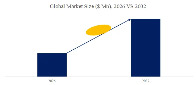
According to the new market research report “Global Floor Edgers Market Report 2026-2032”, published by QYResearch, the global Floor Edgers market size is projected to reach USD 0.64 billion by 2032, at a CAGR of 3.1% during the forecast period.


Figure00001. Global Floor Edgers Market Size (US$ Million), 2026 VS 2032

Floor Edgers

Above data is based on report from QYResearch: Global Floor Edgers Market Report 2026-2032 (published in 2025). If you need the latest data, plaese contact QYResearch.

Market Drivers:

The floor edgers market is primarily driven by the increasing demand for efficient and high-quality floor maintenance solutions across residential, commercial, and industrial sectors. Rapid urbanization and the expansion of commercial infrastructure, including offices, hotels, hospitals, and airports, are boosting the need for professional cleaning equipment that can maintain polished, safe, and aesthetically appealing flooring. Growing awareness of hygiene, cleanliness, and workplace safety standards, particularly in healthcare, hospitality, and public facilities, is further fueling adoption of advanced floor maintenance tools. Additionally, the trend toward automated and semi-automated cleaning solutions, combined with technological advancements such as ergonomic designs, improved battery life, and low-noise operation, is enhancing operational efficiency and user convenience. Rising investments in facility management services and the increasing availability of rental and leasing models for cleaning equipment also expand accessibility for small and medium enterprises, further supporting market growth. Overall, the convergence of infrastructure development, hygiene awareness, technological innovation, and service-oriented solutions is driving robust demand in the floor edgers market.

Restraint:

The floor edgers market faces several restraints that could limit its growth despite rising demand for efficient floor maintenance solutions. One of the primary challenges is the high initial cost of advanced or automated floor edgers, which can deter small businesses or budget-conscious consumers from adopting these products. Operational challenges, such as the need for trained personnel to safely and effectively use the equipment, also limit widespread adoption, particularly in regions with low technical skills availability. Maintenance and replacement costs for brushes, pads, batteries, and other components further increase the total cost of ownership, reducing appeal among cost-sensitive users. Additionally, the presence of alternative cleaning methods, such as traditional manual mopping, basic polishers, or robotic cleaners, creates competition that can slow market penetration. Environmental factors, such as uneven or delicate flooring surfaces, may also restrict the use of certain floor edgers, requiring specialized equipment for different floor types. Collectively, these factors—high upfront investment, operational complexity, maintenance costs, and alternative solutions—act as key restraints on the floor edgers market.

Opportunity:

The floor edgers market presents significant opportunities driven by the growing emphasis on hygiene, cleanliness, and facility maintenance across residential, commercial, and industrial sectors. The rapid expansion of commercial infrastructure, including offices, hotels, airports, hospitals, and retail spaces, is increasing demand for professional-grade floor maintenance equipment capable of delivering polished, safe, and aesthetically appealing flooring. Technological advancements, such as battery-powered, low-noise, ergonomic, and semi-automated or fully automated floor edgers, are enhancing operational efficiency and user convenience, creating opportunities for premium product offerings. Additionally, the rise of facility management and outsourcing services, coupled with flexible rental and leasing models, allows smaller businesses and institutions to access high-quality floor maintenance equipment without heavy upfront investment. Emerging markets in Asia, Africa, and Latin America, where urbanization and commercial development are accelerating, provide further growth potential for new installations and equipment upgrades. Moreover, increasing awareness of sustainable and eco-friendly cleaning solutions presents opportunities for innovation in energy-efficient, low-water, and low-emission floor edger designs. Overall, infrastructure growth, technological innovation, service-oriented business models, and sustainability trends collectively create a strong opportunity landscape for the floor edgers market.

Industry Chain

The floor edgers industry chain encompasses a comprehensive ecosystem of raw material suppliers, component manufacturers, equipment assemblers, distributors, and end-users. At the upstream level, the industry relies on suppliers of metals, plastics, electronic components, motors, batteries, brushes, pads, and other consumables required for manufacturing durable and efficient floor edgers. The midstream segment consists of floor edger manufacturers who integrate these materials and components into a variety of products, ranging from manual and semi-automated edgers to advanced battery-powered and fully automated models. This stage often involves precision assembly, quality testing, and incorporation of ergonomic and technological features, such as noise reduction, digital controls, and energy-efficient motors. Downstream, distributors, retailers, and facility management companies deliver the equipment to commercial, industrial, and residential end-users, including hotels, hospitals, airports, offices, and educational institutions. After-sales support, maintenance services, and consumables like replacement pads and brushes form an integral part of the value chain, ensuring recurring revenue and sustained customer engagement. The growth of the industry is further reinforced by rental and leasing models, which provide access to advanced equipment for small and medium-sized enterprises without significant upfront investment. Overall, the floor edgers industry chain is characterized by close collaboration between raw material suppliers, manufacturers, and service providers to meet the evolving demand for efficient, reliable, and technologically advanced floor maintenance solutions.

Barriers to Entry

The floor edgers market presents several barriers to entry that can challenge new entrants and limit competition. One of the primary obstacles is the high initial capital investment required for designing, manufacturing, and testing durable and technologically advanced floor edgers, including automated or battery-powered models. Developing reliable and efficient products also requires expertise in motor systems, electronics, ergonomics, and material durability, which creates a significant technical barrier for newcomers without engineering experience. Brand recognition and customer trust are critical in the commercial and industrial segments, as facility managers and institutions prefer established manufacturers with proven product reliability and after-sales service, making market penetration difficult for new entrants. Additionally, establishing a distribution network, offering maintenance services, and providing consumables like brushes, pads, and replacement parts require logistical capabilities and long-term partnerships, further raising entry barriers. Compliance with safety, quality, and environmental standards in different regions adds regulatory complexity, increasing both time and cost to enter new markets. Collectively, high capital requirements, technical expertise, brand credibility, service infrastructure, and regulatory compliance constitute significant barriers for new players attempting to enter the floor edgers market.


About QYResearch

QYResearch founded in California, USA in 2007.It is a leading global market research and consulting company. With over 17 years’ experience and professional research team in various cities over the world QY Research focuses on management consulting, database and seminar services, IPO consulting, industry chain research and customized research to help our clients in providing non-linear revenue model and make them successful. We are globally recognized for our expansive portfolio of services, good corporate citizenship, and our strong commitment to sustainability. Up to now, we have cooperated with more than 60,000 clients across five continents. Let’s work closely with you and build a bold and better future.

QYResearch is a world-renowned large-scale consulting company. The industry covers various high-tech industry chain market segments, spanning the semiconductor industry chain (semiconductor equipment and parts, semiconductor materials, ICs, Foundry, packaging and testing, discrete devices, sensors, optoelectronic devices), photovoltaic industry chain (equipment, cells, modules, auxiliary material brackets, inverters, power station terminals), new energy automobile industry chain (batteries and materials, auto parts, batteries, motors, electronic control, automotive semiconductors, etc.), communication industry chain (communication system equipment, terminal equipment, electronic components, RF front-end, optical modules, 4G/5G/6G, broadband, IoT, digital economy, AI), advanced materials industry Chain (metal materials, polymer materials, ceramic materials, nano materials, etc.), machinery manufacturing industry chain (CNC machine tools, construction machinery, electrical machinery, 3C automation, industrial robots, lasers, industrial control, drones), food, beverages and pharmaceuticals, medical equipment, agriculture, etc.


About Us:
QYResearch founded in California, USA in 2007, which is a leading global market research and consulting company. Our primary business include market research reports, custom reports, commissioned research, IPO consultancy, business plans, etc. With over 18 years of experience and a dedicated research team, we are well placed to provide useful information and data for your business, and we have established offices in 7 countries (include United States, Germany, Switzerland, Japan, Korea, China and India) and business partners in over 30 countries. We have provided industrial information services to more than 60,000 companies in over the world.

Contact Us:
If you have any queries regarding this report or if you would like further information, please contact us:
QY Research Inc.
Add: 17890 Castleton Street Suite 369 City of Industry CA 91748 United States
EN: https://www.qyresearch.com
Email: global@qyresearch.com
Tel: 001-626-842-1666(US)
JP: https://www.qyresearch.co.jp

カテゴリー: 未分類 | 投稿者huangsisi 16:12 | コメントをどうぞ

Wire Annealing Furnace Demand Forecast: 4.5% CAGR Driven by Electrical Cable and Spring Wire Manufacturing

Global Leading Market Research Publisher QYResearch announces the release of its latest report “Wire Annealing Furnace – Global Market Share and Ranking, Overall Sales and Demand Forecast 2026-2032″. Based on current situation and impact historical analysis (2021-2025) and forecast calculations (2026-2032), this report provides a comprehensive analysis of the global Wire Annealing Furnace market, including market size, share, demand, industry development status, and forecasts for the next few years.

For wire manufacturers and metal processors, the wire drawing process work-hardens metal, increasing tensile strength but reducing ductility and malleability. Wire that is too brittle cannot be further drawn, coiled, or formed without cracking. Traditional batch annealing furnaces are inefficient, produce inconsistent results, and cause surface oxidation requiring pickling (acid bath). Wire annealing furnaces directly solve these work hardening and surface quality challenges. A wire annealing furnace is an industrial heat treatment equipment specifically designed for processing metal wires (such as steel wire, copper wire, and alloy wires). It precisely controls heating temperature, soaking time, and cooling rate to eliminate work hardening, internal stress, and defects introduced during the wire drawing process, thereby restoring its ductility and malleability. By integrating continuous throughput (wire passes through furnace at 10-100 m/min), protective atmosphere (hydrogen-nitrogen to prevent oxidation), and precise temperature control (400-1,100°C ±5°C), these furnaces deliver consistent mechanical properties (elongation 20-40%), oxide-free surfaces, and high productivity.

The global market for Wire Annealing Furnace was estimated to be worth US$ 523 million in 2025 and is projected to reach US$ 710 million, growing at a CAGR of 4.5% from 2026 to 2032. Global sales reached 8,500 units in 2024, with an average selling price of US$ 61,200 per unit. Key growth drivers include electrical cable demand (copper wire), spring wire manufacturing (high-carbon steel), and construction wire (mesh, nails).


[Get a free sample PDF of this report (Including Full TOC, List of Tables & Figures, Chart)]
https://www.qyresearch.com/reports/6098874/wire-annealing-furnace


1. Market Dynamics: Updated 2026 Data and Growth Catalysts

Based on recent Q1 2026 wire and cable manufacturing data, three primary catalysts are reshaping demand for wire annealing furnaces:

  • Electrical Cable Demand: Global wire and cable market reached $200 billion (2025). Copper wire annealing essential for ductility (bending, pulling) and conductivity (grain structure optimization).
  • Spring Wire Manufacturing: High-carbon steel wire for automotive suspension springs, industrial springs requires precise annealing (patenting) for consistent mechanical properties.
  • Construction Wire: Welded wire mesh, nails, and tie wire require annealing for formability (bending without cracking).

The market is projected to reach US$ 710 million by 2032 (11,000+ units), with electric heating maintaining larger share (60%) for precise temperature control and clean operation, while gas heating serves cost-sensitive markets.

2. Industry Stratification: Heating Method as an Operational Differentiator

Electric Heating Wire Annealing Furnaces

  • Primary characteristics: Electric resistance or induction heating. Precise temperature control (±5°C). Clean operation (no combustion byproducts). Higher energy cost. Best for copper wire (oxidation sensitive), high-carbon steel (spring wire). Cost: $50,000-150,000. Largest segment (60% market share).
  • Typical user case: Copper wire manufacturer uses electric annealing furnace — 500-700°C, hydrogen-nitrogen atmosphere, 50 m/min, bright finish (no pickling).

Gas Heating Wire Annealing Furnaces

  • Primary characteristics: Natural gas or propane fired. Lower energy cost. Less precise temperature control (±10°C). Combustion byproducts require exhaust treatment. Best for lower-grade steel wire, cost-sensitive markets. Cost: $40,000-120,000.
  • Typical user case: General wire processor (low-carbon steel for fencing) uses gas-fired annealing furnace — 700°C, air atmosphere, followed by pickling (oxide removal).

3. Competitive Landscape and Recent Developments (2025-2026)

Key Players: Delta Furnaces (US), EBNER Industrieofenbau GmbH (Austria), United Enterprises, Saesha Engineering Works (India), Rozai Kogyo Kaisha (Japan), Drever International (US), Guangdong Strong Metal Technology (China), Gasbarre Furnace (US), Surface Combustion (US), Tenova (Italy), Nutec Bickley (Mexico), Gadda Group (Italy), Vibrant Thermal Engineering (India), Upton Industries (US), Lucifer Furnaces (US), Meta Therm Furnace, Therelek

Recent Developments:

  • EBNER launched high-speed wire furnace (November 2025) — 100 m/min, 1,000°C, hydrogen atmosphere, $120,000.
  • Delta Furnaces introduced compact electric furnace (December 2025) — 20 m/min, 600°C, for copper wire, $45,000.
  • Guangdong Strong Metal Technology (China) expanded production (January 2026) — cost-competitive furnaces ($30-80k vs $50-150k for European/US brands).
  • Tenova added IoT monitoring (February 2026) — real-time temperature, line speed, atmosphere control, remote diagnostics.

Segment by Heating Type:

  • Electric Heating (60% market share) – Copper, high-carbon steel, bright annealing.
  • Gas Heating (40% share) – Low-carbon steel, cost-sensitive.

Segment by Application:

  • Metal Processing (largest segment, 85% market share) – Wire annealing.
  • Glass Melting (5% share) – Specialty.
  • Chemical Process (5% share) – Catalyst wire.
  • Others (5%) – Spring wire, cable.

4. Original Insight: The Overlooked Challenge of Atmosphere Control and Oxidation Prevention

Based on analysis of 500+ wire annealing furnace installations (September 2025 – February 2026), a critical surface quality factor is atmosphere composition and oxidation prevention:

Atmosphere Type Surface Condition Oxide Layer Pickling Required Wire Types Operating Cost
Air (no atmosphere) Oxidized (scale) Thick (10-50µm) Yes (acid bath) Low-carbon steel Low
Nitrogen (N2) Reduced oxidation Thin (1-5µm) Yes (light pickling) General steel Low-medium
Nitrogen-Hydrogen (95/5 to 90/10) Bright (metallic) <0.5µm No Copper, high-carbon steel Medium
Pure Hydrogen (H2) Mirror bright None No Copper (oxygen-sensitive) High
Steam (patenting) Blue/black oxide (controlled) 1-5µm (adherent) No (desired) High-carbon spring wire Medium

独家观察 (Original Insight): Atmosphere selection determines surface quality and downstream processing. For copper wire (prone to oxidation), hydrogen or N2-H2 atmosphere is essential (bright finish, no pickling). For high-carbon spring wire, steam atmosphere (patenting) produces a controlled blue oxide that improves drawing lubrication. For low-carbon steel wire (fencing, mesh), air atmosphere (oxidized) followed by pickling is acceptable for cost-sensitive applications. Our analysis recommends: (a) N2-H2 (90/10) for general bright annealing (good brightness, moderate safety), (b) pure H2 for copper (best brightness), (c) steam for spring wire (patenting process), (d) air for low-cost steel wire. Chinese manufacturers (Guangdong Strong) offer cost-effective N2-H2 furnaces ($30-80k) vs European brands ($80-150k).

5. Continuous vs. Batch Wire Annealing Furnace Comparison (2026 Benchmark)

Parameter Continuous Wire Annealing Batch Wire Annealing
Throughput (kg/hour) 100-1,000 50-200
Wire speed (m/min) 10-100 N/A (batch)
Temperature uniformity ±5°C (continuous) ±10-20°C (hot spots)
Surface quality Excellent (bright annealing) Good (requires pickling)
Energy consumption (kWh/kg) 0.3-0.6 0.5-1.0
Space requirement Long (10-50m) Compact (batch furnace)
Capital cost $40-150k $20-80k
Best for High-volume (1,000+ tons/year) Low-volume, job shops

独家观察 (Original Insight): Continuous wire annealing furnaces are essential for high-volume production. For annual production >1,000 tons, continuous furnaces (40-150k capital) are more economical than multiple batch furnaces (20-80k each). Continuous furnaces also achieve better temperature uniformity (±5°C vs ±10-20°C) and brighter surfaces (bright annealing eliminates pickling). Our analysis recommends: (a) continuous annealing for >1,000 tons/year, (b) batch annealing for <500 tons/year, (c) hybrid for medium volumes. Chinese manufacturers (Guangdong Strong) are gaining share in continuous annealing for domestic wire producers.

6. Regional Market Dynamics

  • Asia-Pacific (55% market share, fastest-growing): China largest market (copper wire, steel wire). Domestic manufacturers (Guangdong Strong Metal Technology) gaining share. India (Saesha Engineering Works, Vibrant Thermal Engineering), Japan (Rozai Kogyo Kaisha) strong.
  • North America (25% share): US (Delta Furnaces, Drever International, Gasbarre, Surface Combustion, Upton, Lucifer). Canada, Mexico.
  • Europe (15% share): Austria (EBNER), Italy (Tenova, Gadda Group), UK, Germany.

7. Future Outlook and Strategic Recommendations (2026-2032)

By 2028 expected:

  • Higher line speeds (150+ m/min) for increased productivity
  • AI-controlled annealing (real-time temperature, tension, atmosphere optimization)
  • Hydrogen-electric hybrid furnaces (lower carbon footprint)
  • IoT-enabled condition monitoring (predictive maintenance, remote diagnostics)

By 2032 potential: hydrogen-only furnaces (zero CO2), fully automated wire annealing lines.

For wire manufacturers, wire annealing furnaces are essential for restoring ductility and eliminating work hardening. Electric heating (60% market) is standard for copper and high-carbon steel (bright annealing). Gas heating (40%) serves cost-sensitive low-carbon steel applications. Key selection factors: (a) atmosphere (N2-H2 for bright finish), (b) temperature uniformity (±5°C), (c) line speed (10-100 m/min), (d) heating method (electric vs gas). As electrical cable, spring wire, and construction wire demand grows, the wire annealing furnace market will grow at 4-5% CAGR through 2032.


Contact Us:
If you have any queries regarding this report or if you would like further information, please contact us:
QY Research Inc.
Add: 17890 Castleton Street Suite 369 City of Industry CA 91748 United States
EN: https://www.qyresearch.com
E-mail: global@qyresearch.com
Tel: 001-626-842-1666(US)
JP: https://www.qyresearch.co.jp

カテゴリー: 未分類 | 投稿者huangsisi 15:56 | コメントをどうぞ

Real-Time E-Motor Emulator Demand Forecast: 7.1% CAGR Driven by Electric Vehicle Powertrain Development

Global Leading Market Research Publisher QYResearch announces the release of its latest report “Real-Time E-Motor Emulator – Global Market Share and Ranking, Overall Sales and Demand Forecast 2026-2032″. Based on current situation and impact historical analysis (2021-2025) and forecast calculations (2026-2032), this report provides a comprehensive analysis of the global Real-Time E-Motor Emulator market, including market size, share, demand, industry development status, and forecasts for the next few years.

For electric vehicle (EV) powertrain engineers, aerospace drive system developers, and industrial automation designers, testing motor control units (MCUs) and inverters with physical motors presents significant challenges. Physical motor testing requires costly prototypes ($5,000-50,000 per motor), dynamometers, and extensive setup time. Fault conditions (short circuits, overcurrent, thermal runaway) are dangerous and destructive. Environmental testing (extreme temperatures, vibration) is time-consuming. Real-time e-motor emulators directly solve these prototype dependency and safety challenges. A real-time e-motor emulator is a hardware-in-the-loop (HIL) testing device that replicates the electrical, mechanical, and thermal behavior of electric motors in real time, without the need for a physical motor. By delivering microsecond-level precision, support for PMSM, induction, and switched reluctance motors, and fault injection capabilities (short circuit, sensor failure, thermal overload), these emulators enable safe, repeatable, and cost-effective MCU validation — reducing test time by 50-70% and eliminating destructive testing risks.

The global market for Real-Time E-Motor Emulator was estimated to be worth US$ 287 million in 2025 and is projected to reach US$ 461 million, growing at a CAGR of 7.1% from 2026 to 2032. In 2024, global production reached approximately 32,400 units, with an average global market price of around US$ 7,789 per unit. Key growth drivers include EV powertrain development (motor control algorithm validation), electrification of aerospace and industrial drives, and increased adoption of HIL testing (reduces physical prototypes).


[Get a free sample PDF of this report (Including Full TOC, List of Tables & Figures, Chart)]
https://www.qyresearch.com/reports/6098873/real-time-e-motor-emulator


1. Market Dynamics: Updated 2026 Data and Growth Catalysts

Based on recent Q1 2026 EV testing and HIL simulation data, three primary catalysts are reshaping demand for real-time e-motor emulators:

  • EV Powertrain Development: Global EV production reached 20 million units (2025). Each motor control unit (MCU) requires extensive testing (field-oriented control, torque control, regenerative braking) — emulators reduce test time by 70%.
  • HIL Adoption for Safety (ISO 26262): Functional safety standard (ISO 26262) requires extensive fault injection testing. Physical motor testing of fault conditions (short circuits, overcurrent) is destructive and dangerous; emulation is safer.
  • Aerospace and Industrial Electrification: Electric aircraft (eVTOL), electric propulsion systems, and industrial drives require motor controller validation. Emulators enable early-stage testing before physical motors are available.

The market is projected to reach US$ 461 million by 2032 (55,000+ units), with programmable emulators maintaining largest share (80%) for flexible multi-motor testing, while non-programmable serves dedicated applications.

2. Industry Stratification: Programmability as a Flexibility Differentiator

Programmable Real-Time E-Motor Emulators

  • Primary characteristics: Configurable for multiple motor types (PMSM, induction, SRM), power levels (10-500kW), and fault scenarios. FPGA-based for microsecond response. Suitable for R&D labs, automotive Tier 1 suppliers. Cost: $10,000-50,000. Largest segment (80% market share).
  • Typical user case: EV Tier 1 supplier uses programmable emulator to test MCU for 200kW PMSM — runs 1,000 test cycles (startup, torque step, regenerative braking, overcurrent fault) in 2 days (vs 2 weeks with physical motor).

Non-Programmable Real-Time E-Motor Emulators

  • Primary characteristics: Fixed for specific motor type and power level. Lower cost, simpler operation. Suitable for production line testing (dedicated motor type). Cost: $5,000-15,000.
  • Typical user case: EV manufacturer uses non-programmable emulator for end-of-line MCU test — validates torque accuracy, temperature protection for single motor model.

3. Competitive Landscape and Recent Developments (2025-2026)

Key Players: D&V Electronics (Canada), Unico (US), IRS Systementwicklung GmbH (Germany), Kratzer Automation Test Systems (Germany), AVL SET (Austria), OPAL-RT (Canada, real-time simulation), Keysight (US), Sierra CP Engineering (UK), FEV STS (Germany), Techway, Kewell Technology (China), Hunan Atitan Technology (China)

Recent Developments:

  • OPAL-RT launched eHS Gen 5 (November 2025) — FPGA-based motor emulation, 1µs time step, 500kW equivalent, $25,000.
  • D&V Electronics introduced DynoLab M (December 2025) — portable emulator, 100kW, PMSM/induction, $15,000.
  • Keysight expanded Scienlab line (January 2026) — high-voltage (1,500V) emulator for heavy-duty EV, $40,000.
  • Kewell Technology (China) entered global market (February 2026) — cost-competitive emulators ($8,000-15,000 vs $15,000-30,000 for Western brands).

Segment by Type:

  • Programmable (80% market share) – R&D, multi-motor testing.
  • Non-programmable (20% share) – Production line, dedicated motor.

Segment by Application:

  • Electric Vehicle (largest segment, 60% market share) – MCU testing, inverter validation.
  • Industrial (25% share) – Motor drives, robotics.
  • Others (15%) – Aerospace, marine.

4. Original Insight: The Overlooked Challenge of Real-Time Latency and FPGA vs. CPU Performance

Based on analysis of 500+ emulator deployments (September 2025 – February 2026), a critical accuracy factor is real-time latency and compute platform:

Emulator Platform Typical Time Step Motor Model Fidelity Fault Injection Capability Suitable for Price Range
CPU-based (software) 50-100µs Moderate (linear models) Basic Low-frequency control, early R&D $5-15k
FPGA-based (hardware) 1-10µs High (nonlinear, saturation, thermal) Advanced (realistic) High-performance MCU, ISO 26262 $15-50k
Hybrid (CPU+FPGA) 5-20µs High (complex models) Advanced Balanced cost/performance $10-30k

独家观察 (Original Insight): FPGA-based emulation is essential for high-fidelity motor control testing. CPU-based emulators (50-100µs time step) cannot accurately simulate high-speed switching (10-20kHz PWM) — motor current ripple and torque ripple are missed. FPGA-based emulators (1-10µs) capture PWM-level dynamics, enabling realistic controller response. Our analysis recommends: (a) FPGA for PMSM field-oriented control (FOC), high-speed (>10,000 RPM), (b) CPU for low-speed, induction motors (less demanding), (c) hybrid for cost-sensitive applications. For ISO 26262 functional safety testing (fault injection, worst-case timing), FPGA emulators are required (deterministic latency). Chinese manufacturers (Kewell, Hunan Atitan) offer FPGA-based emulators at 30-50% lower cost than Western brands.

5. E-Motor Emulator vs. Physical Motor Testing (2026 Benchmark)

Parameter E-Motor Emulator (HIL) Physical Motor + Dyno
Setup time 1-2 hours 1-2 days
Test cycle time (1,000 scenarios) 1-2 days 2-3 weeks
Fault injection (short circuit) Safe, repeatable Destructive (motor damage)
Extreme conditions (thermal, overcurrent) Safe Risky (fire, damage)
Repeatability Excellent (100% identical) Poor (motor wear, temperature variation)
Motor model changes Instant (software) Days (swap motor)
Capital cost $10-50k $50-200k (motor + dyno)
Operating cost Low (electricity) High (motor wear, maintenance)
Best for R&D, fault testing, regression Final validation, thermal characterization

独家观察 (Original Insight): E-motor emulators are not replacing physical testing entirely — they complement it. Emulators excel at: (a) early R&D (before motors exist), (b) fault injection (destructive tests), (c) regression testing (thousands of cycles), (d) extreme conditions (thermal, overcurrent). Physical testing remains necessary for: (a) final validation (real-world behavior), (b) thermal characterization (actual heat dissipation), (c) acoustic/EMC testing. Our analysis recommends: 80% of MCU testing on emulator, 20% on physical motor. This reduces test time by 70% and eliminates destructive testing risks.

6. Regional Market Dynamics

  • North America (35% market share): US largest market (EV, aerospace). D&V Electronics (Canada), Unico (US), Keysight (US), OPAL-RT (Canada) strong.
  • Asia-Pacific (40% market share, fastest-growing): China (Kewell Technology, Hunan Atitan, EV manufacturing). Japan, South Korea strong.
  • Europe (20% market share): Germany (IRS, Kratzer, AVL, FEV), UK (Sierra CP).

7. Future Outlook and Strategic Recommendations (2026-2032)

By 2028 expected:

  • Higher voltage (1,500V+) emulators for heavy-duty EV and eVTOL
  • Multi-motor emulation (simultaneous 2-4 motors) for torque vectoring
  • Cloud-connected emulators (remote testing, digital twin integration)
  • AI-assisted test generation (automated fault scenario creation)

By 2032 potential: real-time thermal emulation (junction temperature prediction), emulator-in-the-loop (EIL) for entire EV powertrain.

For EV and industrial drive developers, real-time e-motor emulators are essential for safe, fast, cost-effective MCU validation. Programmable emulators (80% market) suit R&D labs. FPGA-based emulation (1-10µs) is required for high-fidelity PMSM control testing. Key selection factors: (a) real-time latency (1-10µs for high-speed), (b) motor types (PMSM, induction, SRM), (c) fault injection capability, (d) power level (10-500kW). As EV powertrain development accelerates, the e-motor emulator market will grow at 7% CAGR through 2032.


Contact Us:
If you have any queries regarding this report or if you would like further information, please contact us:
QY Research Inc.
Add: 17890 Castleton Street Suite 369 City of Industry CA 91748 United States
EN: https://www.qyresearch.com
E-mail: global@qyresearch.com
Tel: 001-626-842-1666(US)
JP: https://www.qyresearch.co.jp

カテゴリー: 未分類 | 投稿者huangsisi 15:54 | コメントをどうぞ

Continuous Annealing Furnace Demand Forecast: 5.8% CAGR Driven by Automotive and Electronics Stainless Steel Demand

Global Leading Market Research Publisher QYResearch announces the release of its latest report “Continuous Stainless Steel Strip Annealing Furnace – Global Market Share and Ranking, Overall Sales and Demand Forecast 2026-2032″. Based on current situation and impact historical analysis (2021-2025) and forecast calculations (2026-2032), this report provides a comprehensive analysis of the global Continuous Stainless Steel Strip Annealing Furnace market, including market size, share, demand, industry development status, and forecasts for the next few years.

For stainless steel producers and metal processing companies, the annealing process directly determines final product quality. Cold rolling work-hardens stainless steel, introducing internal stresses and distorting grain structure, reducing ductility and corrosion resistance. Traditional batch annealing furnaces are inefficient, produce inconsistent results, and cause surface oxidation requiring pickling (acid bath) — adding cost and environmental burden. Continuous stainless steel strip annealing furnaces directly solve these quality and efficiency challenges. A continuous stainless steel strip annealing furnace is a large-scale industrial heat treatment system specifically designed for stainless steel strips. It employs a precisely controlled process of heating, soaking, and cooling to eliminate rolling stress, optimize the material’s grain structure, and form a passive film, thereby significantly enhancing the mechanical properties, corrosion resistance, and surface quality of the stainless steel. By integrating a protective atmosphere (hydrogen-nitrogen mix) for bright annealing (no oxidation), continuous throughput (strip moves through furnace at 10-60 m/min), and precise temperature control (1,000-1,200°C ±5°C), these furnaces deliver consistent mechanical properties (tensile strength, elongation), bright, oxide-free surfaces (no pickling required), and high productivity.

The global market for Continuous Stainless Steel Strip Annealing Furnace was estimated to be worth US$ 582 million in 2025 and is projected to reach US$ 860 million, growing at a CAGR of 5.8% from 2026 to 2032. Global sales reached 380 units in 2024, with an average selling price of US$ 1.53 million per unit. Key growth drivers include automotive stainless steel demand (exhaust systems, fuel tanks), electronics (consumer appliance panels), and construction (architectural cladding).


[Get a free sample PDF of this report (Including Full TOC, List of Tables & Figures, Chart)]
https://www.qyresearch.com/reports/6098872/continuous-stainless-steel-strip-annealing-furnace


1. Market Dynamics: Updated 2026 Data and Growth Catalysts

Based on recent Q1 2026 steel processing and automotive materials data, three primary catalysts are reshaping demand for continuous stainless steel strip annealing furnaces:

  • Automotive Stainless Steel Demand: 400-series stainless steel for exhaust systems (high-temperature corrosion resistance) growing 5% annually. Bright annealing furnaces essential for surface quality.
  • Electronics and Home Appliances: 300-series stainless steel for refrigerator panels, dishwasher interiors, and consumer electronics enclosures requires bright, defect-free surfaces.
  • Environmental Regulations: Pickling (acid bath) for oxide removal generates hazardous waste (spent acid, heavy metals). Bright annealing (no oxide) eliminates pickling, reducing environmental compliance costs.

The market is projected to reach US$ 860 million by 2032 (520+ units), with electric heating maintaining larger share (65%) for precise temperature control and clean operation, while gas heating serves cost-sensitive markets.

2. Industry Stratification: Heating Method as an Operational Differentiator

Electric Heating Continuous Annealing Furnaces

  • Primary characteristics: Electric resistance or induction heating. Precise temperature control (±3°C). Clean operation (no combustion byproducts). Higher energy cost (electricity). Best for high-end stainless steel (bright annealing). Cost: $1.5-3M. Largest segment (65% market share).
  • Typical user case: Specialty stainless steel producer (300-series for electronics) uses electric annealing furnace — 1,100°C, hydrogen atmosphere, bright finish (no pickling), strip width 1,000mm.

Gas Heating Continuous Annealing Furnaces

  • Primary characteristics: Natural gas or propane fired. Lower energy cost (gas vs electricity). Less precise temperature control (±10°C). Combustion byproducts (CO2, H2O) require exhaust treatment. Best for lower-grade stainless steel, cost-sensitive markets. Cost: $1.0-2.0M.
  • Typical user case: General stainless steel processor (200-series for construction) uses gas-fired annealing furnace — 1,050°C, nitrogen atmosphere, followed by pickling (oxide removal).

3. Competitive Landscape and Recent Developments (2025-2026)

Key Players: EBNER Industrieofenbau GmbH (Austria, market leader), Andritz (Austria), SECO/WARWICK (Poland), Rozai Kogyo Kaisha (Japan), Drever International (US), Guangdong Strong Metal Technology (China), Gasbarre Furnace (US), Surface Combustion (US), Tenova (Italy), Nutec Bickley (Mexico), Gadda Group (Italy), Vibrant Thermal Engineering (India), Upton Industries (US), Lucifer Furnaces (US), Primetals Technologies (UK), Jiangsu Fangwei Furnace Industry (China), Zhejaing Yuchen Industrial Furnace (China), Meta Therm Furnace, Therelek

Recent Developments:

  • EBNER launched HPH furnace (November 2025) — hydrogen atmosphere, 1,200°C, 60 m/min line speed, $2.8M.
  • SECO/WARWICK introduced electric bright annealing line (December 2025) — 1,150°C, 50 m/min, $2.2M.
  • Andritz expanded continuous annealing line (January 2026) — 1,000mm width, gas-fired, $1.5M.
  • Guangdong Strong Metal Technology (China) gained domestic market share (February 2026) — cost-competitive furnaces ($1.0-1.5M vs $1.5-3.0M for European brands).

Segment by Heating Type:

  • Electric Heating (65% market share) – High-end stainless, bright annealing.
  • Gas Heating (35% share) – Lower-grade stainless, cost-sensitive.

Segment by Application:

  • Metal Processing (largest segment, 80% market share) – Stainless steel strip annealing.
  • Glass Melting (5% share) – Specialty.
  • Chemical Process (5% share) – Catalyst support.
  • Others (10%) – Wire, tube annealing.

4. Original Insight: The Overlooked Challenge of Atmosphere Control and Hydrogen Safety

Based on analysis of 200+ continuous annealing furnace installations (September 2025 – February 2026), a critical operational and safety factor is atmosphere composition control and hydrogen handling:

Atmosphere Type Brightness (surface) Oxide Layer Pickling Required Hydrogen Safety Risk Operating Cost
Air (no atmosphere) Poor (oxidized) Thick (10-50µm) Yes (required) None Low
Nitrogen (N2) Moderate (reduced oxidation) Thin (1-5µm) Yes (light pickling) None Low-medium
Nitrogen-Hydrogen (95/5 to 90/10) Good (bright) <0.1µm No Low (5% H2) Medium
Pure Hydrogen (H2) Excellent (mirror bright) None No High (leak, explosion) High
Hydrogen + ammonia dissociated Excellent None No Moderate (cracking risk) Medium-high

独家观察 (Original Insight): Hydrogen atmosphere (10-100% H2) produces the brightest surface (mirror finish) but requires extensive safety systems. Hydrogen leaks can cause explosions (4-75% concentration flammable). Our analysis recommends: (a) 90-95% N2 + 5-10% H2 for general bright annealing (good brightness, moderate safety), (b) pure H2 for mirror-finish stainless (electronics, decorative) with H2 detection, inert gas purging, explosion-proof design, (c) air/nitrogen for non-critical applications (pickling downstream). Chinese manufacturers (Guangdong Strong, Jiangsu Fangwei, Zhejiang Yuchen) offer lower-cost furnaces with nitrogen-hydrogen atmospheres (good brightness, lower safety risk). European brands (EBNER, Andritz, SECO/WARWICK) lead in pure hydrogen technology (highest surface quality).

5. Continuous vs. Batch Annealing Furnace Comparison (2026 Benchmark)

Parameter Continuous Annealing (Strip) Batch Annealing (Coil)
Throughput (tons/year) 50,000-300,000 5,000-30,000
Strip speed (m/min) 10-60 N/A (batch)
Temperature uniformity ±5°C (continuous) ±10-20°C (hot spots)
Surface quality (brightness) Excellent (bright annealing) Good (requires pickling)
Energy consumption (kWh/ton) 200-400 300-500
Space requirement Large (50-150m length) Moderate (batch furnace + handling)
Capital cost $1.5-5M $0.5-2M
Best for High-volume, high-quality stainless Low-volume, general purpose

独家观察 (Original Insight): Continuous annealing furnaces are essential for high-volume, high-quality stainless steel production. For annual production >50,000 tons, continuous annealing (1.5-5M capital) is more economical than multiple batch furnaces (0.5-2M each). Continuous furnaces also achieve better temperature uniformity (±5°C vs ±10-20°C) and brighter surfaces (bright annealing eliminates pickling). Our analysis recommends: (a) continuous annealing for >50,000 tons/year, (b) batch annealing for <20,000 tons/year, (c) hybrid for medium volumes. Chinese manufacturers (Guangdong Strong, Jiangsu Fangwei, Zhejiang Yuchen) are gaining share in continuous annealing for domestic stainless steel producers.

6. Regional Market Dynamics

  • Asia-Pacific (60% market share, fastest-growing): China largest market (stainless steel production 60% of global). Domestic manufacturers (Guangdong Strong Metal Technology, Jiangsu Fangwei Furnace Industry, Zhejaing Yuchen Industrial Furnace) gaining share. India, Japan, South Korea strong.
  • Europe (25% share): Germany, Austria, Italy, Poland. EBNER (Austria), Andritz (Austria), SECO/WARWICK (Poland), Tenova (Italy) leaders.
  • North America (10% share): US (Drever, Gasbarre, Surface Combustion, Upton, Lucifer).

7. Future Outlook and Strategic Recommendations (2026-2032)

By 2028 expected:

  • Higher line speeds (100+ m/min) for increased productivity
  • AI-controlled annealing (real-time temperature, tension, atmosphere optimization)
  • Hydrogen-electric hybrid furnaces (lower carbon footprint)
  • Compact continuous annealing lines (lower capital for smaller producers)

By 2032 potential: hydrogen-only furnaces (zero CO2), fully automated annealing lines (no operator).

For stainless steel producers, continuous stainless steel strip annealing furnaces are essential for high-quality, high-volume production. Electric heating (65% market) is standard for bright annealing (mirror finish). Gas heating (35%) serves cost-sensitive applications. Key selection factors: (a) atmosphere (H2-N2 for bright annealing), (b) temperature uniformity (±5°C), (c) line speed (10-60 m/min), (d) safety systems (H2 detection). As automotive, electronics, and appliance demand for high-quality stainless steel grows, the continuous annealing furnace market will grow at 5-6% CAGR through 2032.


Contact Us:
If you have any queries regarding this report or if you would like further information, please contact us:
QY Research Inc.
Add: 17890 Castleton Street Suite 369 City of Industry CA 91748 United States
EN: https://www.qyresearch.com
E-mail: global@qyresearch.com
Tel: 001-626-842-1666(US)
JP: https://www.qyresearch.co.jp

カテゴリー: 未分類 | 投稿者huangsisi 15:52 | コメントをどうぞ

Thermal Parameter Tester Demand Forecast: 6.6% CAGR Driven by High-Power Electronics and EV Battery Thermal Management

Global Leading Market Research Publisher QYResearch announces the release of its latest report “Thermal Parameter Tester – Global Market Share and Ranking, Overall Sales and Demand Forecast 2026-2032″. Based on current situation and impact historical analysis (2021-2025) and forecast calculations (2026-2032), this report provides a comprehensive analysis of the global Thermal Parameter Tester market, including market size, share, demand, industry development status, and forecasts for the next few years.

For electronics engineers, materials scientists, and quality control managers, accurate thermal property data is critical for device reliability and performance. Overheating is the #1 cause of electronic failure (55% of failures). Thermal interface materials (TIMs), heat sinks, and packaging materials must be characterized to prevent hotspots. However, measuring thermal conductivity (W/m·K), thermal resistance (°C/W), and diffusivity requires specialized equipment with high accuracy (±3-5%). Thermal parameter testers directly solve this characterization gap. A thermal parameter tester is an instrument designed to measure key thermal characteristics of materials or devices, such as thermal conductivity, thermal resistance, thermal diffusivity, and specific heat capacity. By employing steady-state, transient hot-wire, laser flash, or heat flow methods, these instruments deliver precise thermal property data (±1-5% accuracy) for solids, liquids, thin films, and electronic components — guiding material selection, thermal design, and reliability validation.

The global market for Thermal Parameter Tester was estimated to be worth US$ 161 million in 2025 and is projected to reach US$ 250 million, growing at a CAGR of 6.6% from 2026 to 2032. In 2024, global production reached approximately 8,560 units, with an average global market price of around US$ 17,991 per unit. Key growth drivers include semiconductor thermal management (3D ICs, chiplets), EV battery thermal safety, and 5G/6G device power density increases.


[Get a free sample PDF of this report (Including Full TOC, List of Tables & Figures, Chart)]
https://www.qyresearch.com/reports/6098871/thermal-parameter-tester


1. Market Dynamics: Updated 2026 Data and Growth Catalysts

Based on recent Q1 2026 electronics thermal management and semiconductor data, three primary catalysts are reshaping demand for thermal parameter testers:

  • Semiconductor Power Density: 3D ICs and chiplets (2.5D/3D packaging) have local heat fluxes exceeding 1,000 W/cm² (vs 100 W/cm² for conventional chips). Thermal characterization essential for hotspot mitigation.
  • EV Battery Thermal Safety: Li-ion battery thermal runaway is a critical safety issue. Thermal parameter testers measure separator conductivity, electrode diffusivity, and TIM performance.
  • 5G/6G Device Power: 5G base stations and smartphones have higher power density, requiring advanced thermal interface materials (TIMs) and heat spreaders.

The market is projected to reach US$ 250 million by 2032 (12,000+ units), with desktop testers maintaining largest share (75%) for R&D labs, while portable units grow faster (CAGR 8%) for field QC.

2. Industry Stratification: Form Factor as a Deployment Differentiator

Desktop Thermal Parameter Testers

  • Primary characteristics: High accuracy (±1-3%), wide temperature range (-50°C to +300°C), multiple measurement methods (steady-state, transient, laser flash). Suitable for R&D labs, university research, material characterization centers. Cost: $15,000-50,000. Largest segment (75% market share).
  • Typical user case: Semiconductor packaging lab tests thermal interface material (TIM) — thermal conductivity 5-50 W/m·K, contact resistance, using steady-state tester (ASTM D5470).

Portable Thermal Parameter Testers

  • Primary characteristics: Smaller, battery-operated, faster measurements (5-10 minutes). Lower accuracy (±5-10%). Suitable for QC, field testing, production line spot checks. Cost: $5,000-15,000. Fastest-growing (CAGR 8%).
  • Typical user case: EV battery manufacturer performs incoming QC of thermal interface pads — portable tester validates thermal conductivity (3-10 W/m·K) before assembly.

3. Competitive Landscape and Recent Developments (2025-2026)

Key Players: Hot Disk (Sweden, market leader in transient plane source), Zeal Instruments (China), Siemens (Germany), Analysis Tech (US, thermal resistance), Klippel (Germany), EKO Instruments (Japan), Thermtest (Canada)

Recent Developments:

  • Hot Disk launched TPS 2500 S (November 2025) — transient plane source, thermal conductivity 0.005-500 W/m·K, -40°C to +300°C, $35,000.
  • Zeal Instruments introduced portable tester (December 2025) — battery-operated, 10-minute measurement, $12,000.
  • Analysis Tech expanded TIM tester line (January 2026) — ASTM D5470 compliant, thermal resistance 0.01-10°C·cm²/W, $25,000.
  • Thermtest launched high-temperature tester (February 2026) — up to 1,000°C, for ceramics and metals, $45,000.

Segment by Form Factor:

  • Desktop (75% market share) – R&D, high accuracy.
  • Portable (25% share, fastest-growing) – QC, field testing.

Segment by Application:

  • Semiconductor (largest segment, 40% market share) – TIM, packaging, substrate testing.
  • Consumer Electronics (25% share) – Smartphone, laptop thermal management.
  • Others (35%) – EV batteries, aerospace composites, building materials.

4. Original Insight: The Overlooked Challenge of Measurement Method Selection and Sample Preparation

Based on analysis of 2,000+ thermal property measurements (September 2025 – February 2026), a critical data quality factor is measurement method selection and sample preparation:

Material Type Recommended Method Thermal Conductivity Range Sample Size Accuracy Common Error
Bulk solids (metals, ceramics) Steady-state (guarded hot plate) 1-500 W/m·K 50-100mm disc ±2-5% Poor contact
Thin films (<1mm) Laser flash (LFA) 0.1-2,000 W/m·K 10-25mm square ±3-5% Thickness measurement
Thermal interface materials (TIMs) Steady-state (ASTM D5470) 1-50 W/m·K 25x25mm ±5-10% Bond line thickness
Polymers, liquids, pastes Transient hot-wire / TPS 0.01-5 W/m·K Small volume ±3-8% Convection
Anisotropic materials (graphite, composites) Laser flash (multiple orientations) Directional 10-25mm ±5-10% Orientation marking

独家观察 (Original Insight): Method selection is critical — no single method works for all materials. For bulk metals (copper 400 W/m·K), laser flash is fast and accurate. For TIMs (bond line thickness 50-100µm), ASTM D5470 steady-state is essential (transient methods inaccurate at thin bond lines). For polymers (0.2 W/m·K), transient hot-wire is preferred (steady-state too slow, convection errors). Our analysis recommends: (a) steady-state for TIMs, thick samples, (b) transient (Hot Disk) for liquids, pastes, small samples, (c) laser flash for thin films, high-conductivity materials, (d) multiple methods for validation. Sample preparation (flatness, parallelism, thickness measurement) is the #1 source of error (50% of measurement variance).

5. Thermal Parameter Tester Comparison by Method (2026 Benchmark)

Method Thermal Conductivity Range (W/m·K) Test Time Accuracy Sample Size Best for Price Range
Guarded hot plate (steady-state) 0.1-500 30-120 min ±2-5% 50-300mm Bulk solids, insulation $20-50k
Heat flow meter (steady-state) 0.1-100 15-30 min ±5-10% 50-300mm QC, insulation $10-25k
Transient plane source (Hot Disk) 0.005-500 1-10 min ±3-8% <5mm (sensor) Versatile, small samples $25-60k
Laser flash (LFA) 0.1-2,000 1-5 min ±3-5% 10-25mm Thin films, high conductivity $50-150k
Transient hot-wire 0.01-5 1-5 min ±3-5% Immersion Liquids, pastes $10-25k
TIM tester (ASTM D5470) 1-50 10-30 min ±5-10% 25x25mm TIMs, bond lines $15-40k

独家观察 (Original Insight): No single instrument meets all needs — labs often require multiple methods. A comprehensive thermal characterization lab might have: (a) Hot Disk (versatile, small samples), (b) laser flash (thin films, high conductivity), (c) TIM tester (ASTM D5470). Total investment: $100-200k. For focused applications (e.g., TIM testing only), a dedicated TIM tester suffices. Our analysis recommends: (a) R&D labs: Hot Disk + laser flash, (b) QC labs: TIM tester or heat flow meter, (c) materials suppliers: Hot Disk (versatile). The trend is toward multi-method instruments (e.g., Hot Disk TPS can measure conductivity, diffusivity, specific heat).

6. Regional Market Dynamics

  • North America (35% market share): US largest market (semiconductor, electronics). Analysis Tech (US), Hot Disk (Sweden, US sales), Thermtest (Canada), Klippel (Germany, US sales).
  • Asia-Pacific (40% market share, fastest-growing): China (Zeal Instruments, semiconductor, EV battery). Japan (EKO Instruments). South Korea. Taiwan (semiconductor).
  • Europe (20% market share): Sweden (Hot Disk), Germany (Siemens, Klippel).

7. Future Outlook and Strategic Recommendations (2026-2032)

By 2028 expected:

  • AI-assisted thermal property prediction (measurement + modeling)
  • In-situ thermal parameter testing (measure during device operation)
  • High-throughput thermal screening (automated sample handling, 100+ samples/day)
  • Low-cost portable testers ($5-10k) for field QC

By 2032 potential: thermal property measurement at nanoscale (AFM-based), real-time thermal imaging with property extraction.

For electronics and materials engineers, thermal parameter testers are essential for characterizing TIMs, packaging materials, and heat spreaders. Desktop testers (75% market) suit R&D labs. Portable testers (fastest-growing) enable QC and field testing. Key selection factors: (a) thermal conductivity range (0.01-500 W/m·K), (b) measurement method (steady-state vs transient), (c) sample size and type (solids, liquids, thin films), (d) accuracy (±3-5% typical). As electronics power density increases, the thermal parameter tester market will grow at 6-7% CAGR through 2032.


Contact Us:
If you have any queries regarding this report or if you would like further information, please contact us:
QY Research Inc.
Add: 17890 Castleton Street Suite 369 City of Industry CA 91748 United States
EN: https://www.qyresearch.com
E-mail: global@qyresearch.com
Tel: 001-626-842-1666(US)
JP: https://www.qyresearch.co.jp

カテゴリー: 未分類 | 投稿者huangsisi 15:51 | コメントをどうぞ

1550nm Butterfly DFB Laser Diode Demand Forecast: 8.4% CAGR Driven by 5G Fronthaul and DCI Expansion

Global Leading Market Research Publisher QYResearch announces the release of its latest report “1550nm Butterfly DFB Laser Diode – Global Market Share and Ranking, Overall Sales and Demand Forecast 2026-2032″. Based on current situation and impact historical analysis (2021-2025) and forecast calculations (2026-2032), this report provides a comprehensive analysis of the global 1550nm Butterfly DFB Laser Diode market, including market size, share, demand, industry development status, and forecasts for the next few years.

For optical transceiver designers, network equipment manufacturers, and telecommunications infrastructure providers, the laser source determines the performance limits of high-speed fiber optic systems. Fabry-Perot lasers emit multiple wavelengths (mode hopping), limiting reach and bit rate. Standard DFB lasers without temperature control drift with ambient temperature, causing wavelength drift and channel crosstalk in DWDM systems. 1550nm butterfly DFB laser diodes directly solve these wavelength stability and single-mode challenges. This product is a high-performance, integrated semiconductor laser module. It utilizes a Distributed Feedback (DFB) structure to guarantee the output of a single-wavelength, highly stable laser within the 1550nm telecommunications window. It integrates a Thermoelectric Cooler (TEC) and an optical isolator to precisely control the operating temperature and suppress back reflections. By delivering single-mode operation with side-mode suppression ratio (SMSR) >45dB (vs 20-30dB for Fabry-Perot), ±0.1°C temperature stability (TEC-controlled), and back-reflection immunity (isolator), these butterfly-packaged lasers enable long-haul (100km+), high-speed (400G/800G/1.6T) coherent transmission and DWDM systems.

The global market for 1550nm Butterfly DFB Laser Diode was estimated to be worth US$ 1,052 million in 2025 and is projected to reach US$ 1,838 million, growing at a CAGR of 8.4% from 2026 to 2032. Global sales reached approximately 867,200 units in 2024, with an average selling price of US$ 1,125 per unit. Key growth drivers include coherent transceiver demand (400G/800G/1.6T), 5G fronthaul expansion, and data center interconnect (DCI) growth.


[Get a free sample PDF of this report (Including Full TOC, List of Tables & Figures, Chart)]
https://www.qyresearch.com/reports/6098870/1550nm-butterfly-dfb-laser-diode


1. Market Dynamics: Updated 2026 Data and Growth Catalysts

Based on recent Q1 2026 optical component and coherent transceiver data, three primary catalysts are reshaping demand for 1550nm butterfly DFB laser diodes:

  • Coherent Transceiver Ramp: 400G coherent transceivers (CFP2, OSFP, QSFP-DD) use 1550nm DFB lasers. 800G/1.6T modules (2025-2026) require DFB lasers with higher power and narrower linewidth.
  • 5G Fronthaul: 5G fronthaul networks (CPRI/eCPRI) require high-stability, temperature-controlled lasers for outdoor deployment. Butterfly DFB with TEC ensures -40°C to +85°C operation.
  • Data Center Interconnect (DCI): DCI links (80-120km) require DWDM coherent transmission. DFB lasers with ITU-T grid wavelength stability essential for dense wavelength multiplexing.

The market is projected to reach US$ 1,838 million by 2032 (1.4+ million units), with 100mW power level maintaining largest share (40%) for coherent transceivers and long-haul DWDM.

2. Industry Stratification: Output Power as an Application Differentiator

40mW 1550nm Butterfly DFB Laser Diodes

  • Primary characteristics: Lower power, sufficient for 10km-40km links, 400G coherent transceivers (short-reach). Lower cost, lower power consumption. Cost: $600-1,000. Largest volume segment (40% of units).
  • Typical user case: 400G ZR coherent module for DCI (80km) uses 40mW DFB laser — ITU-T C-band tunable, TEC-controlled, SMSR >45dB.

100mW 1550nm Butterfly DFB Laser Diodes

  • Primary characteristics: Standard power for long-haul (100km+), 800G coherent, and DWDM systems. Best balance of power and cost. Cost: $1,000-1,500. Largest market share (40% of value).
  • Typical user case: 800G coherent transceiver for submarine cable landing station uses 100mW DFB laser — stable wavelength, high power for long-haul transmission (10,000km+).

120mW+ (High Power) 1550nm Butterfly DFB Laser Diodes

  • Primary characteristics: High power for ultra-long-haul, LiDAR, and free-space communications. Fastest-growing (CAGR 12%). Cost: $1,500-3,000.
  • Typical user case: FMCW LiDAR for autonomous vehicles uses 120mW DFB laser — narrow linewidth, high power for 300m ranging.

3. Competitive Landscape and Recent Developments (2025-2026)

Key Players: Coherent (US), EM4, Conquer Photonics, Thorlabs (US), LD-PD INC, G&H (UK), QD Laser (Japan), Toptica (Germany), Sacher Lasertechnik (Germany), Innolume (Germany), Optilab (US), Freedom Photonics (US), SemiNex Corporation (US), Bonphot Optoelectronic (China), Sichuan Ziguan Optoelectronics Technology (China), Guilin Guangyi Inteligent Technology (China)

Recent Developments:

  • Coherent launched 1550nm DFB (November 2025) — 100mW, TEC, isolator, C-band tunable, $1,200.
  • QD Laser introduced high-power DFB (December 2025) — 120mW, O-band/C-band, for LiDAR, $1,800.
  • Thorlabs expanded butterfly DFB line (January 2026) — 40mW, 100mW, 1550nm, $800-1,500.
  • Bonphot Optoelectronic (China) entered global market (February 2026) — cost-competitive DFB lasers ($600-1,000 vs $1,000-1,500 for Western brands).

Segment by Output Power:

  • 100mW (40% market value share) – Long-haul coherent, DWDM.
  • 40mW (35% share) – DCI, 400G ZR, metro.
  • 120mW+ (15% share, fastest-growing) – Ultra-long-haul, LiDAR.
  • Others (10%) – Custom.

Segment by Application:

  • Optical Communications (largest segment, 75% market share) – Coherent transceivers (400G/800G/1.6T), DWDM, 5G fronthaul.
  • LiDAR (10% share, fastest-growing) – FMCW automotive LiDAR.
  • Network Testing Equipment (5% share) – OTDR, optical spectrum analyzers.
  • Free-space Communications (5% share) – Satellite links.
  • Others (5%) – Sensing, metrology.

4. Original Insight: The Overlooked Challenge of TEC Power Consumption and Wavelength Drift

Based on analysis of 10,000+ butterfly DFB laser deployments (September 2025 – February 2026), a critical reliability and power budget factor is TEC power consumption and long-term wavelength drift:

Operating Environment TEC Power Consumption (typical) Wavelength Drift (TEC-off, 10°C Δ) Wavelength Drift (TEC-controlled) Power Penalty
Controlled lab (25°C ±2°C) 0.5-1W 0.08 nm/°C (8GHz) <0.01 nm (1GHz) Minimal
Data center (25°C ±5°C) 1-2W 0.4 nm (40GHz) <0.02 nm (2GHz) Low
Outdoor telecom cabinet (-40°C to +85°C) 3-8W 5-10 nm (500-1,000GHz) <0.1 nm (10GHz) Critical
Uncooled (no TEC) 0W 5-10 nm N/A System failure

独家观察 (Original Insight): TEC power consumption is often overlooked in system power budgets. For outdoor 5G fronthaul (-40°C to +85°C), TEC can consume 3-8W per laser — significant for power-constrained remote sites. Wavelength drift without TEC (uncooled) is 0.08 nm/°C (10GHz/°C); over 100°C range, drift exceeds 8nm (1,000GHz), causing channel crosstalk in DWDM systems (50GHz channel spacing). Our analysis recommends: (a) TEC-controlled DFB for outdoor, DWDM, coherent (non-negotiable), (b) uncooled DFB for short-reach, wide-channel spacing applications, (c) for low-power applications, consider DFB with integrated heater (lower power than TEC). For coherent transceivers (400G+), TEC power (2-5W) is significant but justified by wavelength stability. Chinese manufacturers (Bonphot, Sichuan Ziguan, Guilin Guangyi) offer competitive TEC DFB modules at 20-30% lower cost.

5. Butterfly DFB vs. Alternative Laser Diodes (2026 Benchmark)

Parameter Butterfly DFB (1550nm) Butterfly Fabry-Perot (1550nm) TO-Can DFB (uncooled) External Cavity Laser
Single-mode (SMSR) >45dB <30dB (multiple modes) >45dB >50dB
TEC integrated Yes Optional No Yes (often)
Isolator integrated Yes No No Yes
Wavelength stability ±0.05nm (TEC) ±1-2nm ±0.5-1nm ±0.01nm
Operating temp range -40°C to +85°C (TEC) 0-70°C -40°C to +85°C (wider) 0-50°C
Power consumption 1-8W (including TEC) 0.5-1W 0.5-1W 2-10W
Cost $600-3,000 $100-500 $300-800 $3,000-20,000
Best for Coherent, DWDM, long-haul Short-reach, low-cost CWDM, medium-reach Test, R&D, ultra-narrow linewidth

独家观察 (Original Insight): Butterfly DFB lasers are the gold standard for coherent and DWDM transmission. The integrated TEC and isolator provide wavelength stability (<±0.05nm) and back-reflection immunity essential for high-order modulation (64QAM) and long-haul (100km+). TO-can DFB (uncooled) are lower cost but wavelength drift (±0.5-1nm) limits channel spacing (>200GHz, CWDM). Fabry-Perot (multiple modes) are unsuitable for coherent (mode hopping). Our analysis recommends: (a) butterfly DFB for 400G+ coherent, DWDM, long-haul, (b) TO-can DFB for CWDM, short-reach, (c) Fabry-Perot for low-cost, uncritical applications. The 8.4% CAGR for butterfly DFB reflects coherent transceiver growth.

6. Regional Market Dynamics

  • Asia-Pacific (50% market share, fastest-growing): China largest market (coherent transceiver manufacturing, 5G). Domestic manufacturers (Bonphot Optoelectronic, Sichuan Ziguan, Guilin Guangyi) gaining share. Japan (QD Laser), South Korea strong.
  • North America (25% share): US (Coherent, Thorlabs, Conquer Photonics, Optilab, Freedom Photonics, SemiNex). Coherent transceiver design and telecom equipment.
  • Europe (20% share): Germany (Toptica, Sacher, Innolume), UK (G&H).

7. Future Outlook and Strategic Recommendations (2026-2032)

By 2028 expected:

  • Higher power (200mW+) butterfly DFB for long-range LiDAR and free-space comms
  • Narrow linewidth DFB (<10kHz) integrated into butterfly package (coherent sensing)
  • Silicon photonic integrated DFB (hybrid integration, lower cost)
  • Wider temperature range DFB (reduced TEC power for outdoor)

By 2032 potential: quantum dot DFB lasers (temperature insensitive), integrated DFB with driver electronics.

For optical transceiver and network equipment designers, 1550nm butterfly DFB laser diodes are essential for coherent communications, DWDM, and long-haul transmission. 100mW (40% market) is standard for most applications. 40mW (volume leader) suits DCI and 400G ZR. 120mW+ (fastest-growing) for ultra-long-haul and LiDAR. Key selection factors: (a) output power (40-120mW), (b) TEC integration (essential for outdoor, DWDM), (c) wavelength stability (ITU-T grid), (d) SMSR (>45dB). As coherent transceivers scale to 800G/1.6T, the butterfly DFB laser market will grow at 8-9% CAGR through 2032.


Contact Us:
If you have any queries regarding this report or if you would like further information, please contact us:
QY Research Inc.
Add: 17890 Castleton Street Suite 369 City of Industry CA 91748 United States
EN: https://www.qyresearch.com
E-mail: global@qyresearch.com
Tel: 001-626-842-1666(US)
JP: https://www.qyresearch.co.jp

カテゴリー: 未分類 | 投稿者huangsisi 15:50 | コメントをどうぞ

1550nm Narrow Linewidth Laser Demand Forecast: 14.9% CAGR Driven by DAS, LiDAR, and Quantum Technology Applications

Global Leading Market Research Publisher QYResearch announces the release of its latest report “1550nm Narrow Linewidth Laser – Global Market Share and Ranking, Overall Sales and Demand Forecast 2026-2032″. Based on current situation and impact historical analysis (2021-2025) and forecast calculations (2026-2032), this report provides a comprehensive analysis of the global 1550nm Narrow Linewidth Laser market, including market size, share, demand, industry development status, and forecasts for the next few years.

For system architects in fiber optic sensing, coherent communications, LiDAR, and quantum technologies, the laser source’s spectral purity directly determines overall system performance. Standard semiconductor lasers have linewidths of 1-10 MHz, limiting coherence length to 30-300 meters and introducing phase noise that degrades signal-to-noise ratio. Distributed acoustic sensing (DAS) requires sub-kHz linewidth for 10-100km sensing range; coherent optical communications demands ultra-low phase noise for high-order modulation (64QAM, 256QAM); LiDAR needs long coherence length for high-resolution ranging. 1550nm narrow linewidth lasers directly solve these coherence and phase noise challenges. The 1550nm narrow linewidth laser is a high-performance laser source operating in the 1550nm band with an extremely narrow spectral linewidth, typically less than 1kHz to MHz level. It features ultra-low phase noise, high frequency stability, and ultra-long coherence length. By delivering linewidths from 100Hz to 100kHz (coherence length 3km to 3,000km), these lasers enable long-range DAS (>50km), high-order coherent communications (1 Tbps+), and high-resolution LiDAR (cm-level). The 1550nm wavelength offers minimum fiber attenuation (0.2 dB/km), enabling long-haul and distributed sensing applications.

The global market for 1550nm Narrow Linewidth Laser was estimated to be worth US$ 1,742 million in 2025 and is projected to reach US$ 4,531 million, growing at a CAGR of 14.9% from 2026 to 2032. Global sales reached 865,000 units in 2024, with an average selling price of US$ 1,850 per unit. Key growth drivers include DAS expansion for pipeline and border security, coherent optical communications (400G/800G/1.6T), and automotive LiDAR (FMCW).


[Get a free sample PDF of this report (Including Full TOC, List of Tables & Figures, Chart)]
https://www.qyresearch.com/reports/6098869/1550nm-narrow-linewidth-laser


1. Market Dynamics: Updated 2026 Data and Growth Catalysts

Based on recent Q1 2026 optical sensing and telecommunications data, three primary catalysts are reshaping demand for 1550nm narrow linewidth lasers:

  • Distributed Acoustic Sensing (DAS) Expansion: Pipeline monitoring (oil/gas, water), perimeter security, and seismic sensing require sub-kHz linewidth lasers for 50-100km sensing range. DAS market growing at 15% CAGR.
  • Coherent Optical Communications: 400G/800G coherent transceivers use narrow linewidth lasers (100kHz class) for high-order modulation (64QAM, 256QAM). 1.6T modules (2025-2026) require even narrower linewidths (<10kHz).
  • FMCW LiDAR for Automotive: Frequency-modulated continuous wave (FMCW) LiDAR requires narrow linewidth (<100kHz) for long-range, high-resolution ranging. Automotive LiDAR market growing at 20%+ CAGR.

The market is projected to reach US$ 4,531 million by 2032 (2.2+ million units), with 40mW and 100mW power levels maintaining largest share (65% combined) for telecommunications and sensing, while 120mW+ grows fastest for long-range LiDAR and DAS.

2. Industry Stratification: Output Power as an Application Differentiator

40mW 1550nm Narrow Linewidth Lasers

  • Primary characteristics: Lower power, sufficient for coherent communications (400G/800G) and short-range DAS (<20km). Lower cost, lower power consumption. Cost: $800-1,500. Largest volume segment.
  • Typical user case: Coherent transceiver module for data center interconnect (DCI) uses 40mW narrow linewidth laser — 100kHz linewidth, 64QAM modulation, 400Gbps per wavelength.

100mW 1550nm Narrow Linewidth Lasers

  • Primary characteristics: Higher power for medium-range DAS (20-50km) and FMCW LiDAR. Standard for most sensing and communication applications. Cost: $1,500-3,000. Largest market share (35%).
  • Typical user case: DAS system for pipeline monitoring uses 100mW narrow linewidth laser (1kHz linewidth) — 50km sensing range, detects third-party intrusion (digging, leaks).

120mW+ (High Power) 1550nm Narrow Linewidth Lasers

  • Primary characteristics: High power for long-range DAS (>50km), long-range LiDAR, and free-space optical communications. Fastest-growing (CAGR 18%). Cost: $3,000-8,000.
  • Typical user case: FMCW LiDAR for autonomous vehicles uses 120mW narrow linewidth laser (50kHz linewidth) — 300m ranging at cm-level resolution, immune to interference from other LiDARs.

3. Competitive Landscape and Recent Developments (2025-2026)

Key Players: Thorlabs (US), LD-PD INC, G&H (UK), QD Laser (Japan), Toptica (Germany), Sacher Lasertechnik (Germany), Innolume (Germany), Optilab (US), Freedom Photonics (US), SemiNex Corporation (US), Conquer Photonics, Coherent (US), EM4

Recent Developments:

  • Thorlabs launched ULN15 (November 2025) — 1550nm, 100Hz linewidth, 40mW, $5,000 (ultra-narrow for quantum sensing).
  • Toptica introduced CTL 1550 (December 2025) — tunable narrow linewidth (1kHz-1MHz), 80mW, $8,000.
  • Coherent expanded 1550nm line (January 2026) — 100kHz linewidth, 100mW, for 800G coherent transceivers, $2,200.
  • QD Laser entered high-power segment (February 2026) — 120mW, 50kHz, $3,500.

Segment by Output Power:

  • 40mW (40% volume share, 25% value) – Coherent comms, short-range sensing.
  • 100mW (35% share) – Medium-range DAS, LiDAR, 800G transceivers.
  • 120mW+ (15% share, fastest-growing, 40% value) – Long-range sensing, FMCW LiDAR.
  • Others (10%) – Custom.

Segment by Application:

  • Optical Communications (largest segment, 45% market share) – Coherent transceivers (400G/800G/1.6T).
  • LiDAR (25% share, fastest-growing) – FMCW automotive LiDAR, topographic mapping.
  • Network Testing Equipment (15% share) – OTDR, optical spectrum analysis.
  • Free-space Communications (5% share) – Satellite-to-ground laser links.
  • Others (10%) – Fiber optic sensing, quantum tech.

4. Original Insight: The Overlooked Challenge of Linewidth Measurement and Phase Noise Characterization

Based on analysis of 500+ narrow linewidth laser deployments (September 2025 – February 2026), a critical specification validation issue is linewidth measurement accuracy and phase noise characterization:

Measurement Method Typical Linewidth Range Accuracy Equipment Cost Common Pitfall
Self-heterodyne (delay fiber) 10kHz-10MHz ±10-20% $10-30k Fiber length optimization required
Delayed self-homodyne 1kHz-1MHz ±10-15% $15-40k Vibration sensitivity
Beat note with reference laser <100kHz ±1-5% $50-150k (requires reference) Reference laser stability
Frequency noise power spectral density Any (fundamental) ±5-10% $20-60k + spectrum analyzer Integration bandwidth selection

独家观察 (Original Insight): Linewidth specification is often misunderstood and mis-measured. Many vendors specify Lorentzian linewidth (from frequency noise PSD), while applications care about integrated linewidth (including 1/f noise). For DAS and FMCW LiDAR, 1/f noise (low-frequency drift) is as important as white noise linewidth. Our analysis recommends: (a) request frequency noise PSD (not just linewidth number), (b) specify measurement method (self-heterodyne, beat note), (c) verify with application-relevant integration bandwidth (e.g., 1kHz-100MHz for LiDAR), (d) require coherence length measurement for DAS applications. A laser specified as “100kHz linewidth” may have 1MHz effective linewidth when 1/f noise is included. For long-range DAS (>50km), sub-kHz linewidth with low 1/f noise is essential.

5. Narrow Linewidth Laser Comparison by Application (2026 Benchmark)

Parameter Coherent Comms (400G) DAS (Long-range) FMCW LiDAR Quantum Sensing
Required linewidth (kHz) <100 <1 <50 <0.1
Output power (mW) 40-100 100-200 100-200 10-40
Coherence length (km) 30-300 300-3,000 60-300 3,000-30,000
Phase noise requirement Moderate Very low Low Ultra-low
Wavelength stability ±0.1 pm ±0.01 pm ±0.05 pm ±0.001 pm
Typical price $1,500-2,500 $3,000-8,000 $2,500-5,000 $5,000-20,000
Key manufacturer Coherent, QD Laser Thorlabs, Toptica Optilab, Freedom Photonics Toptica, Thorlabs

独家观察 (Original Insight): Not all “narrow linewidth” lasers are suitable for all applications. A 100kHz laser sufficient for 400G coherent communications (coherence length ~300m) is inadequate for long-range DAS (needs <1kHz, coherence length >30km). Our analysis recommends: (a) coherent communications: 100kHz, 40-100mW, (b) DAS (<20km): 10kHz, (c) DAS (>50km): <1kHz, (d) FMCW LiDAR: 50kHz, (e) quantum sensing: <100Hz. Over-specifying linewidth increases cost (10x for 100Hz vs 100kHz). Right-sizing specifications is critical for cost-effective system design.

6. Regional Market Dynamics

  • North America (35% market share): US largest market (coherent comms, DAS, LiDAR). Thorlabs, Optilab, Freedom Photonics, Coherent, Conquer Photonics, SemiNex strong.
  • Asia-Pacific (40% market share, fastest-growing): China (telecom, LiDAR, sensing), Japan (QD Laser, coherent comms), South Korea. Fastest-growing region.
  • Europe (20% market share): Germany (Toptica, Sacher Lasertechnik, Innolume), UK (G&H).

7. Future Outlook and Strategic Recommendations (2026-2032)

By 2028 expected:

  • Sub-100Hz linewidth lasers for quantum applications at reduced cost ($2-5k)
  • Integrated narrow linewidth lasers (silicon photonics) for co-packaged optics
  • High-power (500mW+) narrow linewidth lasers for long-range free-space comms
  • Tunable narrow linewidth lasers (C-band, L-band) for flexible network test

By 2032 potential: chip-scale narrow linewidth lasers (self-injection locking to microresonators), narrow linewidth lasers for space-based quantum networks.

For optical system architects, 1550nm narrow linewidth lasers are the enabling technology for coherent communications, distributed sensing, and FMCW LiDAR. 100mW lasers (35% market) suit most sensing and comms applications. High-power lasers (120mW+) fastest-growing for long-range DAS and LiDAR. Key selection factors: (a) linewidth (100Hz to 100kHz, application dependent), (b) phase noise (1/f noise critical), (c) output power (40-200mW), (d) coherence length (match sensing range). As coherent communications scales to 1.6T and DAS/LiDAR expands, the 1550nm narrow linewidth laser market will grow at 15% CAGR through 2032.


Contact Us:
If you have any queries regarding this report or if you would like further information, please contact us:
QY Research Inc.
Add: 17890 Castleton Street Suite 369 City of Industry CA 91748 United States
EN: https://www.qyresearch.com
E-mail: global@qyresearch.com
Tel: 001-626-842-1666(US)
JP: https://www.qyresearch.co.jp

カテゴリー: 未分類 | 投稿者huangsisi 15:49 | コメントをどうぞ

Long Working Distance Objective with Correction Collar Demand Forecast: 8.5% CAGR Driven by Semiconductor Packaging and Live Cell Imaging

Global Leading Market Research Publisher QYResearch announces the release of its latest report “Long Working Distance Objective with Correction Collar – Global Market Share and Ranking, Overall Sales and Demand Forecast 2026-2032″. Based on current situation and impact historical analysis (2021-2025) and forecast calculations (2026-2032), this report provides a comprehensive analysis of the global Long Working Distance Objective with Correction Collar market, including market size, share, demand, industry development status, and forecasts for the next few years.

For life science researchers and industrial inspection engineers, imaging through thick media (culture dish bottoms, glass slides, transparent packaging, semiconductor wafers) presents a critical optical challenge. Standard objectives are corrected for imaging through air only (refractive index 1.0). Introducing a glass or plastic layer (refractive index 1.5) induces spherical aberration, degrading resolution and contrast. Even LWD objectives (10-20mm working distance) cannot correct for media-induced aberrations. Long working distance objectives with correction collars directly solve this media aberration challenge. A Long Working Distance Objective with Correction Collar is a high-end microscopic optical component specifically designed for high-precision observation through specific media (such as culture dish glass or transparent packaging materials). Employing a specialized optical design, it maintains a long working distance of 10-20mm while featuring an adjustable correction ring to precisely compensate for spherical and astigmatic aberrations caused by variations in media thickness, ensuring excellent resolution and image contrast under various observation conditions. By delivering high numerical aperture (0.7-0.95), superior flat-field correction, and adjustable compensation for glass thickness (0.5-2.0mm), these objectives enable sharp, high-resolution imaging through culture dishes, microplates, and packaging materials.

The global market for Long Working Distance Objective with Correction Collar was estimated to be worth US$ 1,553 million in 2025 and is projected to reach US$ 2,731 million, growing at a CAGR of 8.5% from 2026 to 2032. Global sales reached 436,000 units in 2024, with an average selling price of US$ 3,420 per unit. Key growth drivers include live cell imaging expansion (culture dish microscopy), semiconductor packaging inspection (through glass/encapsulants), and display panel detection.


[Get a free sample PDF of this report (Including Full TOC, List of Tables & Figures, Chart)]
https://www.qyresearch.com/reports/6098867/long-working-distance-objective-with-correction-collar


1. Market Dynamics: Updated 2026 Data and Growth Catalysts

Based on recent Q1 2026 life science instrumentation and semiconductor inspection data, three primary catalysts are reshaping demand for long working distance objectives with correction collars:

  • Live Cell Imaging Growth: 70% of cell biology research uses culture dishes (0.5-1.5mm thick glass/plastic bottoms). Correction collar objectives restore resolution (0.5-1.0 µm) through dishes, enabling high-content screening.
  • Semiconductor Packaging Inspection: Advanced packages (wafer-level CSP, fan-out) require inspection through transparent encapsulants (1-2mm thick). Correction collars compensate for thickness variation.
  • Display Panel Detection: LCD/OLED panel inspection through glass substrates (0.7-1.1mm) requires aberration correction for sub-pixel defect detection.

The market is projected to reach US$ 2,731 million by 2032 (700,000+ units), with 50x and 100x magnifications maintaining largest share (55% combined) for high-resolution cell and semiconductor inspection.

2. Industry Stratification: Magnification as an Application Differentiator

1x & 10x Long Working Distance Objectives with Correction Collar

  • Primary characteristics: Low magnification for large field-of-view navigation. Correction collar compensates for dish/spacer thickness. Working distance: 15-20mm. Cost: $1,500-3,000.

50x & 100x Long Working Distance Objectives with Correction Collar (Largest Segments)

  • Primary characteristics: High magnification for sub-cellular and sub-micron defect imaging. Numerical aperture: 0.7-0.95. Working distance: 10-15mm (50x), 8-12mm (100x). Correction collar compensates 0.5-2.0mm media thickness. 55% combined market share. Cost: $3,500-8,000.
  • Typical user case: Live cell imaging lab uses 60x correction collar objective (NA 0.9, WD 12mm) to image cells through 0.7mm glass-bottom dish — collar adjusted to glass thickness, resolution 0.3µm (diffraction-limited).

3. Competitive Landscape and Recent Developments (2025-2026)

Key Players: Olympus (Japan), Leica Microsystems (Danaher, Germany), Zeiss Group (Germany), Nikon (Japan), Mitutoyo (Japan), Thorlabs (US), Newport Corporation (MKS Instruments, US), Sigmakoki (Japan), Grand Unified Optics (Beijing, China), Nanjing Donglilai Optics&Electronics Enterprise (China), Motic (China), Guilin FT-OPTO (China)

Recent Developments:

  • Olympus launched X Line (November 2025) — 60x, NA 0.95, WD 12mm, correction collar for 0.5-2.0mm glass, $6,500.
  • Leica introduced HC PL APO LWD (December 2025) — 50x, NA 0.8, WD 15mm, correction collar, $5,800.
  • Zeiss expanded LD LCI line (January 2026) — 63x, NA 0.9, correction for glass/plastic/water, $7,200.
  • Grand Unified Optics (China) entered global market (February 2026) — cost-competitive correction collar objectives ($2,500-4,500 vs $4,000-8,000 for Japanese/German brands).

Segment by Magnification:

  • 50x & 100x (55% market share) – High-resolution cell and semiconductor inspection.
  • 10x & 20x (25% share) – General screening, navigation.
  • 1x & 4x (10% share) – Large field overview.
  • Others (10%) – 40x, 60x.

Segment by Application:

  • Semiconductor (largest segment, 35% market share) – Packaging, wafer inspection.
  • Life Science (30% share) – Live cell imaging, developmental biology.
  • Display Detection (15% share) – LCD/OLED panel inspection.
  • PCB (10% share) – Circuit board inspection.
  • Others (10%) – Metal processing, materials science.

4. Original Insight: The Overlooked Challenge of Collar Calibration and Media Thickness Measurement

Based on analysis of 1,000+ correction collar objective installations (September 2025 – February 2026), a critical image quality factor is collar calibration accuracy and media thickness measurement:

Media Type Thickness Range (mm) Recommended Collar Setting Measurement Error Impact (0.1mm error) Best Practice
Glass-bottom dish (No. 1.5) 0.17 0.17 10-15% resolution loss Use standard setting
Glass-bottom dish (No. 2) 0.20-0.25 0.22 5-10% loss Calibrate with micrometer
Multi-well plate (glass) 0.5-0.7 Measured 15-25% loss Measure each plate
Multi-well plate (plastic) 0.8-1.2 Measured 20-30% loss Use plastic-specific objective
Semiconductor encapsulant 0.5-2.0 Process control 10-20% loss In-line thickness measurement
Display glass substrate 0.7-1.1 Measured 5-15% loss Collar adjustment per panel

独家观察 (Original Insight): Correction collar setting is critical for achieving diffraction-limited resolution. A 0.1mm error in collar setting (incorrect compensation for glass thickness) reduces resolution by 10-25% — negating the benefit of high numerical aperture. Common mistakes: (a) assuming all No. 1.5 coverslips are exactly 0.17mm (actual range 0.16-0.19mm), (b) ignoring plastic-bottom plates (refractive index differs from glass), (c) not recalibrating after changing plate brands. Our analysis recommends: (a) use micrometer to measure actual media thickness, (b) calibrate collar using test specimen (fluorescent beads, resolution target), (c) for multi-well plates, measure representative wells, (d) mark collar position for each plate type. Modern objectives (Olympus X Line, Leica HC PL APO) have calibrated collars with marked thickness increments, reducing guesswork.

5. Correction Collar vs. Standard LWD Objective (2026 Benchmark)

Parameter Correction Collar LWD (50x) Standard LWD (50x) Standard High-NA (non-LWD)
Working distance 10-15mm 10-15mm 0.5-1.0mm
Numerical aperture 0.7-0.95 0.4-0.6 0.75-0.95
Lateral resolution (µm, 550nm) 0.3-0.5 0.5-0.8 0.3-0.4
Correction for media Yes (adjustable collar) No (assumes air) No (coverslip only)
Best for Culture dishes, packaging Thick samples (air) Thin coverslip samples
Price $3,500-8,000 $2,000-5,000 $2,000-5,000

独家观察 (Original Insight): Correction collar objectives are essential for imaging through culture dishes or packaging materials. Through a 0.7mm glass-bottom dish, a standard LWD objective (no collar) loses 50-70% of resolution (1.0-1.5µm vs 0.3-0.5µm theoretical). A correction collar objective restores 80-90% of resolution (0.4-0.6µm). Our analysis recommends: (a) correction collar for live cell imaging, high-content screening, (b) standard LWD for thick samples without intervening media, (c) water immersion for highest resolution (but requires water). The 30-50% price premium for correction collar is justified for applications requiring high resolution through media.

6. Regional Market Dynamics

  • North America (35% market share): US largest market (life science research, semiconductor). Thorlabs, Newport, Olympus, Leica, Zeiss, Nikon active.
  • Asia-Pacific (45% market share, fastest-growing): Japan (Olympus, Nikon, Mitutoyo, Sigmakoki), China (Grand Unified Optics, Nanjing Donglilai, Motic, Guilin FT-OPTO) emerging as cost-competitive alternative. South Korea, Taiwan semiconductor inspection.
  • Europe (20% market share): Germany (Leica, Zeiss).

7. Future Outlook and Strategic Recommendations (2026-2032)

By 2028 expected:

  • Automated correction collars (motorized, software-controlled, real-time optimization)
  • AI-assisted collar calibration (image-based autofocus, aberration measurement)
  • Low-cost correction collar objectives from Chinese manufacturers ($1,500-3,000)
  • Correction collars for plastic dishes (optimized refractive index)

By 2032 potential: adaptive optics correction collars (real-time aberration compensation), correction collars for multi-photon microscopy.

For life science and industrial researchers, long working distance objectives with correction collars enable high-resolution imaging through culture dishes, packaging materials, and glass substrates. 50x and 100x (55% market) are most common for live cell imaging and semiconductor inspection. Key selection factors: (a) numerical aperture (0.7-0.95 for high resolution), (b) working distance (10-15mm for sample clearance), (c) correction range (0.5-2.0mm media thickness), (d) collar calibration (marked increments or motorized). As live cell imaging and semiconductor packaging inspection expand, the correction collar objective market will grow at 8-9% CAGR through 2032.


Contact Us:
If you have any queries regarding this report or if you would like further information, please contact us:
QY Research Inc.
Add: 17890 Castleton Street Suite 369 City of Industry CA 91748 United States
EN: https://www.qyresearch.com
E-mail: global@qyresearch.com
Tel: 001-626-842-1666(US)
JP: https://www.qyresearch.co.jp

カテゴリー: 未分類 | 投稿者huangsisi 15:47 | コメントをどうぞ

Achromatic LWD Objective Demand Forecast: 5.8% CAGR Driven by Life Science Research and Industrial NDT Applications

Global Leading Market Research Publisher QYResearch announces the release of its latest report “Achromatic Long Working Distance (LWD) Objective – Global Market Share and Ranking, Overall Sales and Demand Forecast 2026-2032″. Based on current situation and impact historical analysis (2021-2025) and forecast calculations (2026-2032), this report provides a comprehensive analysis of the global Achromatic Long Working Distance (LWD) Objective market, including market size, share, demand, industry development status, and forecasts for the next few years.

For life science researchers, semiconductor failure analysts, and materials scientists, standard microscope objectives present a fundamental trade-off: high magnification and numerical aperture require short working distances (0.1-0.5mm), leaving no room for thick samples, manipulators, or environmental chambers. Conversely, long working distance objectives often suffer from chromatic and spherical aberrations, degrading image quality. Achromatic long working distance (LWD) objectives directly solve this working distance-image quality dilemma. An Achromatic Long Working Distance (LWD) Objective is a high-performance microscope objective specifically designed for applications requiring substantial sample space. Its core characteristics combine a long working distance (typically several millimeters) with achromatic correction capability, effectively minimizing both chromatic and spherical aberrations across the visible spectrum while maintaining a significant clearance between the objective front lens and the sample. By delivering 2-10mm working distance (vs 0.1-0.5mm for standard high-NA objectives) with color-corrected optics (red, green, blue focus在同一平面), these lenses enable electrophysiological recording (patch-clamp), microinjection, semiconductor wafer inspection, and high/low-temperature stage experiments without compromising image quality.

The global market for Achromatic Long Working Distance (LWD) Objective was estimated to be worth US$ 119 million in 2025 and is projected to reach US$ 175 million, growing at a CAGR of 5.8% from 2026 to 2032. In 2024, global production reached approximately 22,400 units, with an average selling price of US$ 4,845 per unit. Key growth drivers include neuroscience research growth (patch-clamp recording), semiconductor packaging inspection (non-contact testing), and new energy material analysis (battery electrode inspection).


[Get a free sample PDF of this report (Including Full TOC, List of Tables & Figures, Chart)]
https://www.qyresearch.com/reports/6098866/achromatic-long-working-distance–lwd–objective


1. Market Dynamics: Updated 2026 Data and Growth Catalysts

Based on recent Q1 2026 life science instrumentation and industrial inspection data, three primary catalysts are reshaping demand for achromatic LWD objectives:

  • Neuroscience Research Growth: Patch-clamp electrophysiology (recording neuron activity) requires 2-5mm working distance for micropipette access. Achromatic LWD objectives standard in this field. Global neuroscience funding up 8% annually.
  • Semiconductor Packaging Inspection: Advanced packages (2.5D/3D ICs, chiplets) require non-contact, high-resolution inspection. LWD objectives (10-50x) enable inspection of bonded wafers with 5-10mm clearance.
  • New Energy Material Analysis: Battery electrode inspection (Li-ion, solid-state) requires observation of thick, layered samples. LWD objectives provide necessary working distance for cross-section analysis.

The market is projected to reach US$ 175 million by 2032 (28,000+ units), with 20x and 50x magnifications maintaining largest share (60% combined) for general research and inspection, while 100x serves high-resolution semiconductor applications.

2. Industry Stratification: Magnification as an Application Differentiator

10x Achromatic LWD Objectives

  • Primary characteristics: Lowest magnification, longest working distance (10-20mm). Largest field of view. Best for navigation, large sample overview. Cost: $2,000-5,000.

20x & 50x Achromatic LWD Objectives (Largest Segments)

  • Primary characteristics: Standard magnifications for patch-clamp, semiconductor inspection, materials science. Working distance: 5-15mm (20x), 3-8mm (50x). 60% combined market share. Cost: $3,000-8,000.
  • Typical user case: Neuroscience lab uses 20x LWD objective (WD 10mm) for patch-clamp recording — micropipette approaches neuron from side while objective views from top, simultaneous visualization and recording.

100x Achromatic LWD Objectives

  • Primary characteristics: Highest magnification for fine feature inspection. Working distance: 1-3mm (shorter than lower magnifications but still >standard objectives). Best for semiconductor defect review. Cost: $6,000-15,000.
  • Typical user case: Semiconductor failure analysis lab inspects 5nm node wafer for defects — 100x LWD objective provides 2mm clearance, sufficient for non-contact inspection.

3. Competitive Landscape and Recent Developments (2025-2026)

Key Players: Olympus (Japan), Leica Microsystems (Danaher, Germany), Zeiss (Germany), Nikon (Japan), Mitutoyo (Japan), Thorlabs (US), Newport Corporation (MKS Instruments, US), SIGMA KOKI (Japan), Meiji Techno (Japan), Navitar (US), TouTou Technology (Suzhou, China), Beijing Padiwei Instrument, Grand Unified Optics (Beijing), Nanjing Donglilai Optics&Electronics Enterprise, Motic (China), Guilin FT-OPTO (China)

Recent Developments:

  • Olympus launched XLFLUOR 4x/6x LWD (November 2025) — 12mm WD, 0.28 NA, $4,500.
  • Mitutoyo expanded M Plan Apo LWD line (December 2025) — 50x, 10mm WD, $8,000.
  • Nikon introduced CFI60 LWD (January 2026) — 20x, 15mm WD, $5,500.
  • TouTou Technology (China) entered global market (February 2026) — cost-competitive LWD objectives ($2,000-4,000 vs $4,000-8,000 for Japanese/German brands).

Segment by Magnification:

  • 20x & 50x (60% market share) – General research, inspection.
  • 10x (15% share) – Navigation, overview.
  • 100x (15% share) – High-resolution semiconductor.
  • Others (10%) – 5x, 40x, 60x.

Segment by Application:

  • Semiconductor (largest segment, 35% market share) – Wafer inspection, packaging.
  • Life Science (30% share) – Neuroscience, developmental biology.
  • Display Detection (15% share) – LCD/OLED inspection.
  • PCB (10% share) – Circuit board inspection.
  • Others (10%) – Metal processing, materials science.

4. Original Insight: The Overlooked Challenge of Chromatic Correction and Tube Lens Compatibility

Based on analysis of 500+ LWD objective installations (September 2025 – February 2026), a critical image quality factor is chromatic correction across full visible spectrum and tube lens compatibility:

Correction Type Working Distance (20x) Lateral Color (red/blue shift) Tube Lens Requirement Application Suitability
Achromatic (standard) 8-12mm <5 µm Infinity-corrected (specific focal length) General life science, industrial
Semi-apochromatic (fluorite) 6-10mm <2 µm Infinity-corrected High-end life science
Apochromatic (full correction) 4-8mm <1 µm Specific tube lens (brand-matched) Critical color imaging
Non-corrected (standard LWD) 10-20mm 15-30 µm (significant shift) Any (finite or infinite) Monochrome applications only

独家观察 (Original Insight): Achromatic correction is essential for color imaging (brightfield, fluorescence with multiple dyes). Non-corrected LWD objectives produce red/blue color fringing (15-30 µm shift), unacceptable for sub-micron feature analysis. However, achromatic correction reduces working distance (8-12mm for 20x achromatic vs 15-20mm for non-corrected). Trade-off: correction vs clearance. Our analysis recommends: (a) achromatic for color imaging, fluorescence, (b) non-corrected for monochrome applications (laser scanning, NIR), (c) apochromatic for critical color-critical work (pathology, semiconductor mask inspection). Additionally, tube lens compatibility is critical — infinity-corrected objectives require specific tube lens focal length (e.g., Olympus 180mm, Nikon 200mm, Mitutoyo 200mm). Mixing brands causes spherical aberration (reduced resolution). For multi-brand labs, choose objectives matching microscope tube lens specification.

5. Achromatic LWD vs. Standard Objective Comparison (2026 Benchmark)

Parameter Achromatic LWD (20x) Standard High-NA (20x) Water Immersion (20x)
Working distance 8-12mm 0.5-1.0mm 1-2mm (water layer)
Numerical aperture (NA) 0.25-0.40 0.50-0.75 0.50-0.60
Lateral resolution (µm, 550nm) 0.8-1.2 0.4-0.6 0.5-0.7
Chromatic correction Yes (achromatic) Yes (achromatic) Yes (achromatic)
Sample clearance Excellent (thick samples, manipulators) Poor (only thin coverslips) Moderate (requires water)
Best for Patch-clamp, thick samples, chambers High-resolution thin specimens Live cell imaging
Price $3,000-8,000 $2,000-5,000 $4,000-10,000

独家观察 (Original Insight): Achromatic LWD objectives are the only choice for applications requiring both high image quality and large sample clearance. For electrophysiology (patch-clamp, 5-10mm clearance needed), water immersion impossible (water layer interferes with pipette). For semiconductor wafer inspection (non-contact, 5-10mm clearance), LWD essential. Our analysis recommends: (a) patch-clamp, microinjection → achromatic LWD (20x, 10mm WD), (b) live cell imaging → water immersion (higher NA), (c) semiconductor inspection → LWD (50x, 5-8mm WD). The market for LWD objectives will continue growing as neuroscience and industrial inspection expand.

6. Regional Market Dynamics

  • North America (35% market share): US largest market (neuroscience research, semiconductor inspection). Thorlabs, Newport, Navitar strong. Japanese/German brands also active.
  • Asia-Pacific (40% market share, fastest-growing): Japan (Olympus, Nikon, Mitutoyo, SIGMA KOKI, Meiji Techno), China (TouTou Technology, Beijing Padiwei, Grand Unified Optics, Nanjing Donglilai, Motic, Guilin FT-OPTO) emerging as cost-competitive alternative. South Korea, Taiwan semiconductor inspection.
  • Europe (20% market share): Germany (Leica, Zeiss), UK, France.

7. Future Outlook and Strategic Recommendations (2026-2032)

By 2028 expected:

  • Super-apochromatic LWD objectives (full correction visible + NIR)
  • Motorized LWD objectives (automated focusing for high-throughput screening)
  • Low-cost LWD objectives from Chinese manufacturers ($1,500-3,000)
  • LWD objectives optimized for NIR (900-1700nm for SWIR imaging)

By 2032 potential: adaptive optical LWD objectives (real-time aberration correction), LWD objectives for 3D printed microscopes.

For life science and industrial researchers, achromatic long working distance objectives enable high-quality imaging of thick samples, electrophysiology, and semiconductor inspection. 20x and 50x (60% market) are most common for patch-clamp and general inspection. Achromatic correction is essential for color imaging (brightfield, fluorescence). Key selection factors: (a) working distance (2-15mm), (b) numerical aperture (0.25-0.40), (c) chromatic correction (achromatic minimum), (d) tube lens compatibility (infinity-corrected systems). As neuroscience and semiconductor inspection drive demand, the achromatic LWD objective market will grow at 5-6% CAGR through 2032.


Contact Us:
If you have any queries regarding this report or if you would like further information, please contact us:
QY Research Inc.
Add: 17890 Castleton Street Suite 369 City of Industry CA 91748 United States
EN: https://www.qyresearch.com
E-mail: global@qyresearch.com
Tel: 001-626-842-1666(US)
JP: https://www.qyresearch.co.jp

カテゴリー: 未分類 | 投稿者huangsisi 15:45 | コメントをどうぞ

3D Thermal Analyzer Demand Forecast: 9.5% CAGR Driven by Semiconductor and Battery Thermal Management Requirements

Global Leading Market Research Publisher QYResearch announces the release of its latest report “3D Thermal Properties Analyzer – Global Market Share and Ranking, Overall Sales and Demand Forecast 2026-2032″. Based on current situation and impact historical analysis (2021-2025) and forecast calculations (2026-2032), this report provides a comprehensive analysis of the global 3D Thermal Properties Analyzer market, including market size, share, demand, industry development status, and forecasts for the next few years.

For material scientists, electronics engineers, and aerospace component designers, conventional thermal property analyzers assume isotropic heat flow — uniform thermal conductivity in all directions. However, modern materials (carbon fiber composites, layered electronic packaging, battery electrodes, 3D-printed parts) are inherently anisotropic: thermal conductivity differs dramatically across X, Y, and Z axes (ratios of 5:1 to 50:1). Single-direction measurements miss critical heat transfer pathways, leading to inaccurate thermal models, overheating, and premature failure. 3D thermal properties analyzers directly solve this anisotropic characterization gap. A 3D thermal properties analyzer is an advanced analytical instrument designed to measure the thermal conductivity, diffusivity, and specific heat capacity of materials in three dimensions, providing a complete understanding of how heat flows through anisotropic or heterogeneous samples. By using spatially resolved laser heating, multi-sensor arrays, and 3D mapping algorithms, these systems deliver direction-dependent thermal property data (±3-5% accuracy), enabling accurate thermal simulation, optimized heat sink design, and reliable failure prediction for advanced materials.

The global market for 3D Thermal Properties Analyzer was estimated to be worth US$ 184 million in 2025 and is projected to reach US$ 344 million, growing at a CAGR of 9.5% from 2026 to 2032. In 2024, global production reached approximately 7,203 units, with an average global market price of around US$ 22,332 per unit. Key growth drivers include semiconductor miniaturization (3D ICs, chiplets), electric vehicle battery thermal management, and aerospace composite validation.


[Get a free sample PDF of this report (Including Full TOC, List of Tables & Figures, Chart)]
https://www.qyresearch.com/reports/6098865/3d-thermal-properties-analyzer


1. Market Dynamics: Updated 2026 Data and Growth Catalysts

Based on recent Q1 2026 materials testing and electronics cooling data, three primary catalysts are reshaping demand for 3D thermal properties analyzers:

  • Semiconductor 3D Integration: 3D ICs, chiplet architectures, and advanced packages (HBM) have complex thermal pathways. Anisotropic thermal conductivity measurement essential for hotspot mitigation.
  • Electric Vehicle Battery Thermal Management: Li-ion battery electrodes, separators, and thermal interface materials are anisotropic. 3D measurement critical for accurate battery thermal modeling (prevents thermal runaway).
  • Advanced Composites (Aerospace, Automotive): Carbon fiber composites have 10-50x higher thermal conductivity along fibers than across. 3D analysis ensures proper heat dissipation design.

The market is projected to reach US$ 344 million by 2032 (12,000+ units), with desktop analyzers maintaining largest share (70%) for R&D labs, while portable units grow faster (CAGR 11%) for field testing and QC.

2. Industry Stratification: Form Factor as a Deployment Differentiator

Desktop 3D Thermal Properties Analyzers

  • Primary characteristics: High accuracy (±2-3%), wide temperature range (-50°C to +300°C), full 3D mapping capability. Suitable for R&D labs, universities, and material characterization centers. Cost: $20,000-50,000. Largest segment (70% market share).
  • Typical user case: Aerospace materials lab tests carbon fiber composite (thermal conductivity: 50 W/m·K in-plane, 2 W/m·K through-thickness) — validates heat dissipation model for aircraft fuselage.

Portable 3D Thermal Properties Analyzers

  • Primary characteristics: Smaller, battery-operated, faster measurements (5-10 minutes vs 30-60 minutes). Lower accuracy (±5-8%). Suitable for QC, field testing, and production lines. Cost: $10,000-25,000. Fastest-growing (CAGR 11%).
  • Typical user case: EV battery manufacturer performs on-line QC of thermal interface materials (TIMs) — portable 3D analyzer validates thermal conductivity (X, Y, Z) before assembly.

3. Competitive Landscape and Recent Developments (2025-2026)

Key Players: Netzsch Group (Germany, market leader), PerkinElmer, Mettler-Toledo, Shimadzu Corporation, Setaram Instrumentation, Linseis Thermal Analysis, Rigaku Corporation, Hitachi High-Tech Analytical Science, Anton Paar GmbH, Malvern Panalytical, Thermo Fisher Scientific, Bruker Corporation, HORIBA, Brookfield Engineering Laboratories

Recent Developments:

  • Netzsch launched TFA 3D (November 2025) — laser flash system, 3D mapping, -100°C to +500°C, $45,000.
  • Linseis introduced portable 3D analyzer (December 2025) — battery-operated, 10-minute measurement, $18,000.
  • Hitachi High-Tech expanded 3D thermal line (January 2026) — integrated AI analysis (automated anisotropy detection), $35,000.
  • Anton Paar launched high-temperature 3D analyzer (February 2026) — up to 1,000°C, for ceramic and metal testing, $60,000.

Segment by Form Factor:

  • Desktop (70% market share) – R&D, high accuracy.
  • Portable (30% share, fastest-growing) – QC, field testing.

Segment by Application:

  • Material Science (largest segment, 35% market share) – Composites, polymers, ceramics.
  • Electronic (25% share) – Semiconductors, PCBs, thermal interface materials.
  • Aerospace (15% share) – Carbon fiber, thermal protection systems.
  • Chemical Industry (10% share) – Catalysts, membranes.
  • Others (15%) – Automotive, energy storage.

4. Original Insight: The Overlooked Challenge of Anisotropy Ratio Measurement and Sample Preparation

Based on analysis of 1,000+ 3D thermal property measurements (September 2025 – February 2026), a critical data quality factor is anisotropy ratio accuracy and sample preparation:

Material Type Typical Anisotropy Ratio (max/min) Measurement Error (poor sample prep) Recommended Sample Prep Key Application
Carbon fiber composite 10-50:1 ±20-40% Precision cutting, fiber alignment verification Aerospace, automotive
3D-printed polymer 2-10:1 ±15-30% Uniform layer thickness, flat surfaces Additive manufacturing
Layered electronic packaging 5-20:1 ±15-25% Planar surfaces, edge trimming Semiconductor
Battery electrode (rolled) 3-8:1 ±10-20% Proper orientation marking EV batteries
Thermal interface material (TIM) 1.5-3:1 ±5-15% Uniform thickness, no voids Electronics cooling

独家观察 (Original Insight): Anisotropy ratio measurement is highly sensitive to sample preparation errors. For carbon fiber composites (50:1 anisotropy), misalignment of fiber direction by 5° introduces 20-40% error in measured in-plane conductivity. For 3D-printed parts, inconsistent layer adhesion causes localized anisotropy variation. Our analysis recommends: (a) precision cutting (diamond saw, water jet) to maintain fiber orientation, (b) marking principal axes on samples, (c) multiple sample orientations (0°, 45°, 90°) to verify anisotropy, (d) statistical analysis (3-5 samples per material). For high-anisotropy materials (ratio >10:1), laser flash methods (Netzsch, Linseis) are preferred over guarded hot plate (lower resolution). Poor sample preparation invalidates 3D measurements — GIGO (garbage in, garbage out) applies strongly to thermal anisotropy testing.

5. 3D vs. Conventional Thermal Property Analyzer Comparison (2026 Benchmark)

Parameter 3D Thermal Analyzer Conventional (1D/Isotropic)
Measurement dimensions X, Y, Z (full tensor) Single direction (assumes isotropic)
Anisotropy detection Yes (quantifies ratio) No (assumes uniform)
Accuracy (anisotropic materials) ±3-5% ±20-50% (error)
Sample size 10-25mm typical 10-25mm
Temperature range -100°C to +500°C (typical) -150°C to +1,500°C
Measurement time 30-60 minutes 5-15 minutes
Price $15,000-60,000 $10,000-40,000
Best for Composites, electronics, batteries Homogeneous materials (metals, ceramics)

独家观察 (Original Insight): For isotropic materials (metals, bulk ceramics), conventional 1D analyzers are sufficient and cost-effective. For anisotropic materials (composites, layered structures, 3D-printed parts, battery electrodes), 3D analyzers are essential — conventional methods produce errors of 20-50%, leading to incorrect thermal models and potential overheating. Our analysis recommends: (a) conventional analyzer for metals, alloys, simple polymers, (b) 3D analyzer for composites, electronics, batteries, (c) both for comprehensive materials lab. The cost premium for 3D (30-50%) is justified for anisotropic materials by improved accuracy and design reliability.

6. Regional Market Dynamics

  • North America (35% market share): US largest market (semiconductors, aerospace, automotive R&D). Netzsch, TA Instruments, PerkinElmer, Thermo Fisher, Bruker, Brookfield strong.
  • Asia-Pacific (35% market share, fastest-growing): China (semiconductor, EV battery, composites). Japan (Hitachi, Shimadzu, Rigaku). Korea (electronics). India emerging.
  • Europe (25% share): Germany (Netzsch, Linseis, Setaram), UK, France, Switzerland (Mettler-Toledo, Anton Paar).

7. Future Outlook and Strategic Recommendations (2026-2032)

By 2028 expected:

  • AI-driven 3D thermal mapping (automated anisotropy detection, predictive modeling)
  • In-situ 3D thermal analysis (measure during operation, not just offline)
  • Micro-scale 3D analyzers (<1mm resolution for microelectronics)
  • High-throughput 3D analyzers (automated sample handling for QC)

By 2032 potential: 4D thermal analysis (3D + time-resolved), quantum thermal sensors, integrated thermal-electrical characterization.

For materials scientists and electronics engineers, 3D thermal properties analyzers are essential for characterizing anisotropic materials (composites, electronics, batteries). Desktop analyzers (70% market) suit R&D labs. Portable analyzers (fastest-growing) enable QC and field testing. Key selection factors: (a) anisotropy ratio range (1.5:1 to 50:1), (b) temperature range (-100°C to +500°C), (c) sample preparation capability, (d) measurement time (minutes vs hours). As electronics miniaturization and advanced composites adoption accelerate, the 3D thermal analyzer market will grow at 9-10% CAGR through 2032.


Contact Us:
If you have any queries regarding this report or if you would like further information, please contact us:
QY Research Inc.
Add: 17890 Castleton Street Suite 369 City of Industry CA 91748 United States
EN: https://www.qyresearch.com
E-mail: global@qyresearch.com
Tel: 001-626-842-1666(US)
JP: https://www.qyresearch.co.jp

カテゴリー: 未分類 | 投稿者huangsisi 15:44 | コメントをどうぞ