Global Leading Market Research Publisher QYResearch announces the release of its latest report *”Maintenance Optimization Solution – Global Market Share and Ranking, Overall Sales and Demand Forecast 2026-2032″*. Based on current situation and impact historical analysis (2021-2025) and forecast calculations (2026-2032), this report provides a comprehensive analysis of the global Maintenance Optimization Solution market, including market size, share, demand, industry development status, and forecasts for the next few years.
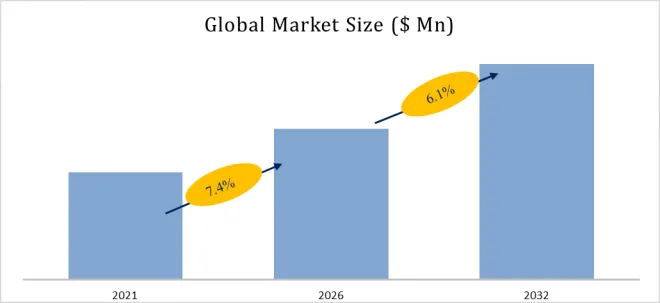
For plant managers, asset reliability engineers, and facility operators, unplanned equipment downtime costs industrial manufacturers an estimated 50billionannually,witheachhourofautomotiveassemblylinestoppagereaching50billionannually,witheachhourofautomotiveassemblylinestoppagereaching1-2 million in lost production. Traditional reactive maintenance (fix after failure) leads to extended downtime and safety risks, while time-based preventive maintenance (scheduled regardless of condition) results in unnecessary part replacements and labor costs. Maintenance optimization solutions directly address these challenges through data-driven, intelligent analysis, and automation technologies that continuously improve maintenance strategies. The core approach shifts organizations from reactive maintenance to predictive maintenance (PdM) and proactive optimization, integrating Internet of Things (IoT), artificial intelligence (AI), and big data analytics to achieve scientific, precise maintenance decision-making – reducing failure rates, extending service life, minimizing downtime, and controlling costs. The global market for Maintenance Optimization Solution was estimated to be worth US518millionin2025andisprojectedtoreachUS518millionin2025andisprojectedtoreachUS 866 million, growing at a CAGR of 7.7% from 2026 to 2032.
【Get a free sample PDF of this report (Including Full TOC, List of Tables & Figures, Chart)
https://www.qyresearch.com/reports/6096112/maintenance-optimization-solution
Understanding Maintenance Optimization: From Reactive to Predictive
Maintenance optimization solutions encompass software platforms (CMMS – computerized maintenance management systems, EAM – enterprise asset management), IoT sensors (vibration, temperature, oil analysis, ultrasonic, thermal imaging), AI/ML analytics (anomaly detection, remaining useful life prediction, failure pattern recognition), and prescriptive analytics (optimized scheduling, resource allocation). Core technologies:
- IoT: Real-time equipment condition monitoring, continuous data collection.
- AI/ML: Pattern recognition (fault signatures), predictive models (time-to-failure), recommendation engines.
- Digital twin: Simulate maintenance strategies, trade-offs.
- Mobile apps: Work order management, technician routing, parts inventory.
Maintenance strategy evolution:
- Reactive (run-to-failure): Lowest upfront cost, highest downtime, safety risks.
- Preventive (time/cycle-based): Reduce unplanned failures, but over-maintenance, waste.
- Predictive (condition-based): Maintain only when indicated, low downtime, optimized.
- Prescriptive (AI-optimized): Combines predictive with resource constraints, job scheduling.
Market Segmentation by Solution Type
- Predictive Maintenance (PdM) Optimization (Dominant, ~40-45% of market value): Condition monitoring using sensors + ML to forecast failures. Algorithms: vibration analysis (FFT, envelope), thermal imaging, oil debris analysis, motor current signature. Use case: wind turbine gearbox failure prediction (weeks advance). Industry: heavy equipment, energy, manufacturing.
- Preventive Maintenance (PM) Optimization (~25-30%): Optimize existing scheduled maintenance intervals (reduce frequency without increasing risk). Uses RCM (reliability-centered maintenance), statistical failure data. CMMS modules.
- Proactive Maintenance Optimization (~15-20%): Root cause failure analysis (RCFA), design improvements, operator training, parts quality upgrades. Eliminate recurring failures long-term.
- Adaptive Maintenance Optimization (~10-15%): Real-time adjusting maintenance schedules based on production demand, spare parts availability, technician workload. Prescriptive analytics.
Market Segmentation by Application
- Industrial Equipment (Largest, ~40-45% of market value): Manufacturing machinery (CNC, injection molding, presses, conveyors, packaging lines), pumps, compressors, HVAC, cranes. Industry 4.0, smart factory. ROI: reduced unplanned downtime 30-50%, maintenance cost 15-30%, extended asset life.
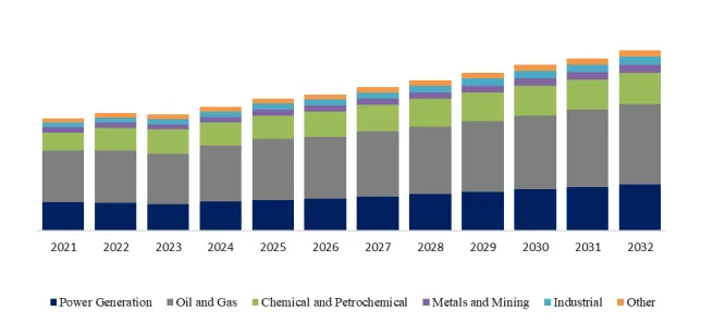
- Energy Facilities (~20-25%): Power generation (gas turbines, wind turbines, solar inverters, nuclear, hydro), oil & gas (refineries, pipelines, offshore platforms). High consequence of failure (safety, environmental, production loss). PdM standard.
- Transportation (~15-20%): Fleet maintenance (trucks, locomotives, aircraft, ships). Predictive for engines, brakes, tires. Rail (wayside detectors). Aviation (gas path analysis).
- Construction (~5-10%): Heavy equipment (excavators, bulldozers, cranes). Telematic data (engine hours, fault codes). Small market.
- Others (Water/wastewater, mining, data centers): Facilities (chillers, UPS, generators). Hospitals (MRI, CT scanners). Smaller.
Competitive Landscape and Exclusive Market Observation (2025–2026)
Key Players: DecisionBrain (France, advanced planning, optimization, PdM for supply chain), GCC Solutions (Netherlands, maintenance software), Baker Hughes (US, oil & gas, Bently Nevada condition monitoring, asset reliability), Elazur (UAE, maintenance management), Fracttal (Spain, CMMS predictive maintenance, cloud), Efor Group (Italy, AI maintenance), ManWinWin Software (Portugal, CMMS), ABL Group (Norway, energy consulting), SEAM Group (US, asset reliability), Keel Solution (France, CMMS), EURODECISION (France, optimization software for maintenance scheduling), Maintenance Innovators (Germany, PdM), Nsflow (Austria, digital maintenance platform), Systecon Group (Sweden, Opus Suite for Life Cycle Management).
Exclusive Industry Insight (H1 2026): Maintenance optimization market is growing rapidly (7.7% CAGR) with cloud-based CMMS and AI PdM adoption:
- Shift from legacy (on-prem CMMS) to cloud/SaaS (lower upfront, automatic updates, mobile access). Fracttal, UpKeep, Fiix, MaintainX (not in list). Traditional vendors (IBM Maximo, SAP) offering cloud.
- AI Predictive analytics moving from niche (high-value assets) to mainstream (general industrial). ML models trained on historical failure data, real-time sensor streams. Reduced false positives (better than threshold-based alarms). Edge AI (gateways compute on site, send only anomalies).
- Industrial IoT sensor costs declining (vibration sensors 100−500vs100−500vs1,000+ 5 years ago). Wireless LPWAN (LoRaWAN, NB-IoT) enabling retrofit of legacy equipment.
User case: Manufacturing plant (automotive, 2025). 500+ critical assets (CNC, presses, conveyors). Implemented Fracttal CMMS + IoT vibration sensors on 50 high-risk assets. Predictive algorithm detected bearing degradation (press) 3 weeks before failure. Scheduled maintenance during planned downtime (avoided $500k production loss). ROI <6 months. Reduced total downtime 28%, maintenance cost 18%.
User case 2: Wind farm (onshore, 100 turbines). Baker Hughes Bently Nevada condition monitoring (vibration, temperature, oil). PdM detects gearbox tooth cracking, bearing wear, generator electrical faults. 8-12 weeks advance warning. Reduced catastrophic failures, extended turbine life. O&M cost savings 15-20%. Industry standard.
Technical Deep Dive: Predictive vs. Preventive Optimization
| Feature | Preventive (PM) | Predictive (PdM) |
|---|---|---|
| Trigger | Time/cycle (e.g., every 1000 hours) | Condition (vibration > threshold) |
| Data | Maintenance history, OEM manuals | Real-time sensor data, ML models |
| Downtime impact | Scheduled, but may be unnecessary | Only when needed |
| Cost | Parts replaced regardless | Parts used only near EOL |
| Implementation | Low (work orders) | High (sensors, analytics) |
| Best for | Low-criticality assets | High-criticality, expensive assets |
Future Outlook (2026–2032): Drivers and Challenges
Growth Drivers:
- Industry 4.0 / smart factory adoption (digital twins, IIoT, AI analytics). Competitive pressure.
- Skilled labor shortage (maintenance technicians retiring). Automation (prescriptive analytics, AI assistants) compensate.
- ESG and sustainability (reduce waste from over-maintenance, energy efficiency).
- Cloud CMMS lower entry barriers (small and medium enterprises adopt).
Constraints:
- Data integration complexity (legacy equipment no sensors, incompatible systems, data quality).
- Change management (organizations resist moving from reactive culture). Training.
- Cybersecurity risk (connected OT systems vulnerable to ransomware – take down facility). IT/OT convergence challenges.
Emerging technologies: Digital twin simulation (test maintenance strategies, predict outcome). Autonomous maintenance (robots performing inspections, basic repairs). Generative AI for work order generation (auto-describe fault, recommend parts, procedure). Computer vision (visual inspection via cameras, detect leaks, cracks, corrosion).
The market projected 7-8% CAGR 2026-2032. Predictive maintenance fastest growing (9-10%). Energy, industrial equipment largest segments. Cloud CMMS displacing legacy on-prem. AI integration key differentiator.
Contact Us
If you have any queries regarding this report or if you would like further information, please contact us:
QY Research Inc.
Add: 17890 Castleton Street Suite 369 City of Industry CA 91748 United States
EN: https://www.qyresearch.com
E-mail: global@qyresearch.com
Tel: 001-626-842-1666 (US)
JP: https://www.qyresearch.co.jp