Global Leading Market Research Publisher QYResearch announces the release of its latest report “High Performance CMOS Image Sensor – Global Market Share and Ranking, Overall Sales and Demand Forecast 2026-2032″. Based on current situation and impact historical analysis (2021-2025) and forecast calculations (2026-2032), this report provides a comprehensive analysis of the global High Performance CMOS Image Sensor market, including market size, share, demand, industry development status, and forecasts for the next few years.
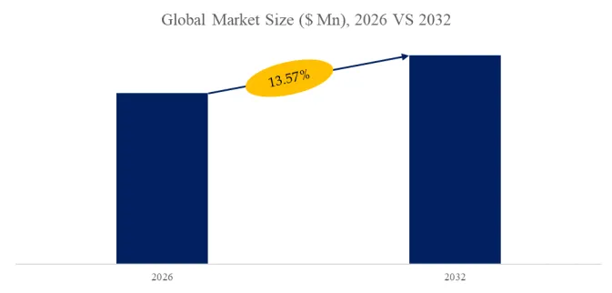
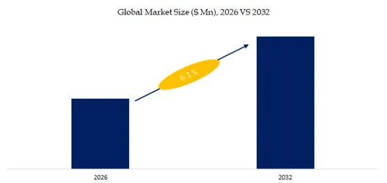
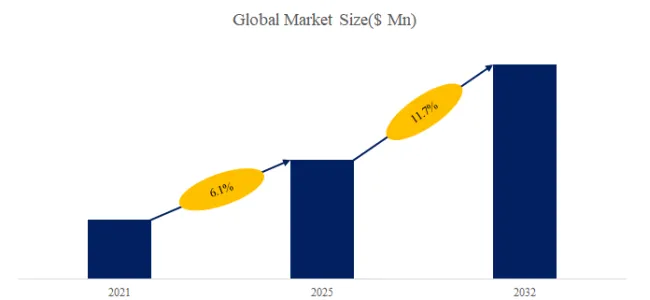
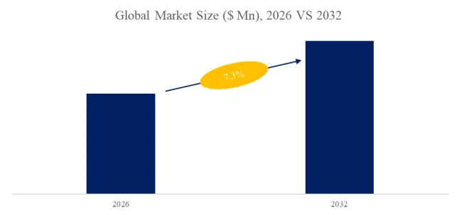
The global market for High Performance CMOS Image Sensor was estimated to be worth US22269millionin2025andisprojectedtoreachUS22269millionin2025andisprojectedtoreachUS 44655 million, growing at a CAGR of 9.9% from 2026 to 2032. In 2025, global High Performance CMOS Image Sensor production reached approximately 7.95 billion units, with an average global market price of around US$ 2.8 per unit. High Performance CMOS Image Sensor (High Performance CIS) refers to a type of CMOS image sensor that has excellent performance in core imaging indicators, and is optimized for scenarios with high requirements for imaging quality, speed, and environmental adaptability. It is different from general-purpose CIS that balances cost and basic performance, and its design focuses on breaking through the limits of imaging performance.
【Get a free sample PDF of this report (Including Full TOC, List of Tables & Figures, Chart)】
https://www.qyresearch.com/reports/5544333/high-performance-cmos-image-sensor
1. Core Market Dynamics: Pixel Architecture Evolution, Automotive ADAS Mandates, and the Resolution vs. Sensitivity Trade-off
Three core keywords define the current competitive landscape of the High Performance CMOS Image Sensor market: stacked BSI (Back-Side Illuminated) architecture, automotive-grade high dynamic range (HDR > 120dB), and wafer-level packaging (WLP) for miniaturization. Unlike general-purpose CIS designed for cost-sensitive consumer applications (smartphones, webcams), high performance CIS addresses critical pain points in demanding scenarios: automotive ADAS (reliable object detection in extreme lighting conditions from direct sunlight to dark tunnels), industrial machine vision (global shutter capture of fast-moving objects without distortion), medical imaging (high signal-to-noise ratio for diagnostic accuracy), and professional photography (extremely high resolution with low noise).
The solution direction for system integrators involves selecting CIS architectures optimized for specific performance parameters rather than general-purpose balanced designs. Back-side illuminated (BSI) technology—where photodiodes are placed above wiring layers rather than below them—increases quantum efficiency (light capture) by 30-50% compared to front-side illuminated (FSI) sensors, enabling smaller pixels without sensitivity loss. Stacked BSI (manufactured by Sony, Samsung, TSMC for OmniVision) adds a separate logic wafer beneath the pixel array, allowing pixel process optimization independent of logic process, enabling features like DRAM integration for high-speed capture and on-chip HDR processing.
2. Segment-by-Segment Analysis: Pixel Architecture and Application Channels
The High Performance CMOS Image Sensor market is segmented as below:
Segment by Type
- Front Side Illuminated (FSI)
- Back Side Illuminated (BSI)
- Stacked CMOS Image Sensor
Segment by Application
- Scientific Research
- Automotive
- Industrial
- Professional Photography
2.1 Pixel Architecture: Performance Tiers and Application Matching
Front Side Illuminated (FSI) sensors (estimated 15-20% of high performance CIS revenue) represent the legacy architecture, where light passes through wiring layers before reaching photodiodes, losing 30-50% of incident photons. FSI remains relevant only for cost-sensitive applications or large-pixel designs (>3µm pixel pitch) where wiring layer obstruction is proportionally smaller. In the high performance category, FSI is increasingly limited to industrial sensors prioritizing global shutter (simultaneous capture across all pixels) over sensitivity.
Back Side Illuminated (BSI) sensors (40-45% share) are the current mainstream for high performance applications, offering quantum efficiency of 80-90% (versus 50-60% for FSI). BSI enables pixel pitch reduction to 1.0-1.2µm without sensitivity loss, supporting high resolution (20-50 megapixels) in compact formats. Key technical challenge: thin wafer handling during manufacturing (backside thinning to 3-5µm) requires specialized equipment and process control, limiting supply to advanced foundries (Sony, Samsung, TSMC). BSI sensors dominate automotive and professional photography applications.
Stacked CMOS Image Sensors (35-40% share) represent the fastest-growing segment (projected CAGR 12-14% from 2026 to 2032), adding a logic wafer bonded to the pixel wafer. This architecture enables: (1) pixel-dedicated process (optimized for sensitivity and dark current) separate from logic process (optimized for speed and power); (2) embedded DRAM for high-speed capture (1,000 fps at full resolution for industrial inspection); (3) on-chip HDR processing (merging multiple exposure frames on-sensor, reducing latency). Sony pioneered stacked CIS with its Exmor RS series; Samsung and OmniVision (manufactured by TSMC) have since introduced competitive stacked products.
2.2 Application Segmentation: Automotive Leads Growth, Scientific Research Commands Highest ASP
Automotive applications represent the fastest-growing segment (projected CAGR 15-17% from 2026 to 2032), driven by ADAS (Advanced Driver Assistance Systems) and autonomous vehicle development. High performance CIS in automotive must meet AEC-Q100 Grade 2 (-40°C to 105°C) or Grade 1 (-40°C to 125°C) certification, with specific requirements: high dynamic range (>120dB to handle tunnel entry/exit lighting extremes), LED flicker mitigation (LED pulsing at 90-120Hz causes false detection in rolling shutter sensors), and functional safety (ISO 26262 ASIL-B or higher). A typical Level 2+ autonomous vehicle uses 8-12 cameras (front-view, rear-view, surround-view, in-cabin monitoring), each requiring automotive-grade CIS. Key customers include Tesla, BYD, Volkswagen, Bosch, Continental, and emerging Chinese EV manufacturers.
Professional photography (25-30% share) demands maximum resolution (50-200 megapixels), largest pixel pitch (3-5µm for maximum light capture), and highest dynamic range (>15 stops). This segment commands the highest average selling prices (15−50persensorversus15−50persensorversus2-5 for automotive, $1-3 for consumer). Key suppliers: Sony (dominates full-frame and medium format sensors for Nikon, Sony Alpha, Fujifilm), Canon (captive manufacturing for EOS series), and Samsung (selected partnership with Phase One, Hasselblad). Market growth is limited by the contraction of dedicated camera sales (CIPA data shows 30% decline from 2015-2025), but ASP increases (transition to higher-resolution sensors) partially offset volume declines.
Industrial applications (20-25% share) include machine vision for manufacturing inspection, robotics guidance, barcode scanning, and semiconductor inspection. Key requirements: global shutter (all pixels capture simultaneously, eliminating distortion for moving objects or strobe lighting), high frame rate (1,000-10,000 fps for high-speed inspection), and monochrome variants (for applications requiring maximum sensitivity without color filter array). ON Semiconductor, Sony, and OmniVision dominate this segment. A case study from a semiconductor wafer inspection equipment manufacturer (Q4 2025) reported that migrating from 5-megapixel rolling shutter sensors to 20-megapixel global shutter stacked CIS increased inspection throughput 3x by eliminating the need for step-and-repeat image stitching.
Scientific research (10-15% share) represents the highest technical specification tier: extreme low noise (less than 2 electrons read noise for astronomy applications), very large pixel pitch (5-10µm for maximum well capacity), specialized spectral response (UV to SWIR, often without Bayer color filter array), and thermoelectric cooling (reducing dark current for long exposures). This segment has the highest ASP ($50-500 per sensor) but lowest volume, with key suppliers including Sony (scientific back-illuminated sensors), ON Semiconductor (interline transfer CCD replacement), and specialized manufacturers like Canons and SOI. Growth drivers include astronomical observatory upgrades (e.g., Rubin Observatory’s 3.2-gigapixel sensor array, completed 2024), fluorescence microscopy, and X-ray imaging.
3. Industry Structure: Vertical Hierarchical Supply Chain with Strong Concentration
The CMOS image sensor industry chain presents a vertical hierarchical structure with clear division of labor, spanning from upstream core material and equipment supply, midstream sensor design, manufacturing and packaging, to downstream application terminal integration.
Upstream: Core Materials & Equipment (Technical Core, High Barriers) – The upstream segment provides essential materials (semiconductor wafers, photoresist, metal targets, packaging materials) and equipment (photolithography scanners from ASML, etching and deposition equipment from Applied Materials and Tokyo Electron). The equipment accounts for a large proportion of CIS production costs, with core links monopolized by overseas enterprises. For advanced stacked CIS, EUV lithography (ASML) is increasingly used for the logic wafer, while the pixel wafer uses deep UV (DUV) lithography.
Midstream: CIS Design, Manufacturing & Packaging (Value Core, High Concentration) – The midstream covers three key links: chip design, wafer fabrication, and packaging/testing. The market concentration is extremely high:
- Design (IDM Mode): Sony Semiconductor Solutions (market leader with 40-45% revenue share), Samsung Electronics (20-25% share), OmniVision (10-15% share). Sony’s advantage lies in proprietary stacked BSI technology (first to commercialize DRAM-integrated stacked CIS). Samsung leverages vertical integration of logic and memory manufacturing. OmniVision (owned by Wingtech Technology) competes through Fabless + TSMC manufacturing.
- Design (Fabless Mode): ON Semiconductor (strong in automotive and industrial), SK Hynix (focusing on mid-range), GalaxyCore (consumer-focused).
- Wafer Fabrication: TSMC (largest foundry, focuses on high-end stacked CIS for OmniVision, Apple), UMC, GlobalFoundries, SMIC (focusing on mid-to-low-end CIS process).
- Packaging & Testing: Advanced packaging (wafer-level packaging, chip-scale packaging) is critical for miniaturization and performance. Leaders include ASE Group, Amkor Technology. Wafer-level packaging reduces sensor size by 40% compared to traditional ceramic packages.
Downstream: Application Terminal Integration (Demand Core, Diversified Scenarios) – Downstream applications include consumer electronics (traditional main market, gradual saturation), automotive electronics (fastest growing), security monitoring (stable demand), and industrial/medical fields (high profit margin, professional demand).
4. Technical Challenges and Innovation Frontiers
Key technical challenges and innovation priorities in the High Performance CMOS Image Sensor market include:
- Pixel size reduction limit: As pixel pitch approaches 0.5-0.7µm, photon shot noise and crosstalk between adjacent pixels degrade image quality regardless of BSI architecture. Industry solutions include: (1) deeper photodiode structures (vertical transfer gates); (2) improved microlens arrays (light focusing into smaller active areas); (3) back-side deep trench isolation (optical crosstalk reduction).
- High dynamic range techniques: Automotive applications require >120dB HDR. Methods include: multiple exposure (fast/slow captures merged), dual conversion gain (switching full-well capacity), split-diode pixels (simultaneous high/low sensitivity captures). Each method involves trade-offs between frame rate, motion artifact, and power consumption.
- Global shutter vs. rolling shutter: Rolling shutter (pixels exposed sequentially) causes distortion for fast-moving objects. Global shutter (simultaneous exposure) requires storage capacitors in each pixel, reducing fill factor (light capture area). Pregius (Sony) and XGS (ON Semi) are leading global shutter pixel designs.
- Near-infrared sensitivity: Enhanced NIR sensitivity (700-1,000nm) benefits automotive night vision, security cameras, and medical imaging. Techniques include thicker silicon epitaxial layers (5-10µm), back-side illumination without color filters, and specialized photodiode structures.
5. Market Forecast and Strategic Outlook (2026-2032)
With a projected CAGR of 9.9% from 2026 to 2032, the High Performance CMOS Image Sensor market exhibits strong growth driven by automotive electrification and autonomous driving, industrial automation, and scientific/medical imaging. Profit concentration: upstream equipment and midstream design links occupy the highest profit margin, while downstream application terminal profit margin is relatively low. Regional concentration: upstream and midstream high-end links are concentrated in Japan, South Korea, United States, and Taiwan of China; downstream application market is dominated by China, the world’s largest CIS consumer market.
Strategic priorities for industry participants include: (1) investment in stacked BSI with DRAM integration for high-speed automotive and industrial applications; (2) development of automotive-grade global shutter sensors for driver monitoring and surround-view systems; (3) expansion of NIR-enhanced sensor product lines for security and medical applications; (4) qualification of additional foundry partners (beyond Sony and Samsung) for supply chain resilience; and (5) pursuit of in-pixel HDR and LED flicker mitigation for Level 3+ autonomous vehicles.
Contact Us:
If you have any queries regarding this report or if you would like further information, please contact us:
QY Research Inc.
Add: 17890 Castleton Street Suite 369 City of Industry CA 91748 United States
EN: https://www.qyresearch.com
E-mail: global@qyresearch.com
Tel: 001-626-842-1666(US)
JP: https://www.qyresearch.co.jp