QY Research Inc. (Global Market Report Research Publisher) announces the release of 2025 latest report “Cockpit Display System for Aerospace- Global Market Share and Ranking, Overall Sales and Demand Forecast 2026-2032”. Based on current situation and impact historical analysis (2020-2024) and forecast calculations (2026-2032), this report provides a comprehensive analysis of the global Cockpit Display System for Aerospace market, including market size, share, demand, industry development status, and forecasts for the next few years.
The global market for Cockpit Display System for Aerospace was estimated to be worth US$ 4536 million in 2025 and is projected to reach US$ 8127 million, growing at a CAGR of 8.5% from 2026 to 2032.
【Get a free sample PDF of this report (Including Full TOC, List of Tables & Figures, Chart)】
https://www.qyresearch.com/reports/5651303/cockpit-display-system-for-aerospace
Product Overview and Scope of Cockpit Display System for Aerospace
Cockpit display systems for aerospace are integrated human-machine interface devices installed in the cockpit of aircraft or spacecraft. They present multi-source information, including flight, navigation, engine, and warning information, to pilots/astronauts in real time in graphical, symbolic, or video format. They typically consist of a Primary Flight Display (PFD), a Multifunction Display (MFD), an Engine Indication and Crew Alarm System (EICAS), and an optional Head-Up Display (HUD), and are a core component of the glass cockpit.
Core raw materials include: aerospace-grade LCD or Micro-LED panels, high-brightness LED backlight arrays, coated electromagnetic shielding glass, carbon fiber/aluminum alloy frames, light guide plates, quantum dot films, FPGA/multi-core GPU image processing modules, ARINC-818/fiber optic video interfaces, and gallium nitride power management ICs. In the cost structure, high-brightness wide-temperature LCD or Micro-LED modules account for 35%–45% of the total BOM, shielding glass and vibration-resistant frame account for 15%–20%, image generation and interface circuits account for 20%–25%, and the remainder is for optical bonding, environmental testing, airworthiness certification, and software V&V. Due to the stringent certification requirements of DO-178C/DO-254 and DO-160, a single 15-in IDU costs $30,000–$50,000, and a complete HUD system (including waveguide, projection, and night vision interface) can reach $100,000–$200,000, making it one of the most expensive LRUs in the cockpit.
Cockpit Display System for Aerospace Market Summary
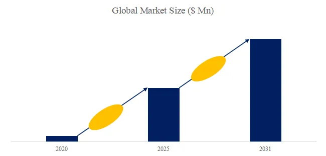
According to the new market research report “Global Cockpit Display System for Aerospace Market Report 2025-2031”, published by QYResearch, the global Cockpit Display System for Aerospace market size is projected to reach USD 7.48 billion by 2031, at a CAGR of 8.2% during the forecast period.
Figure00001. Global Cockpit Display System for Aerospace Market Size (US$ Million), 2020-2031
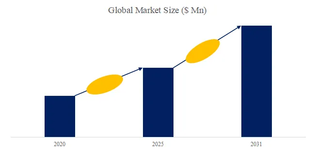
Above data is based on report from QYResearch: Global Cockpit Display System for Aerospace Market Report 2025-2031 (published in 2025). If you need the latest data, plaese contact QYResearch.
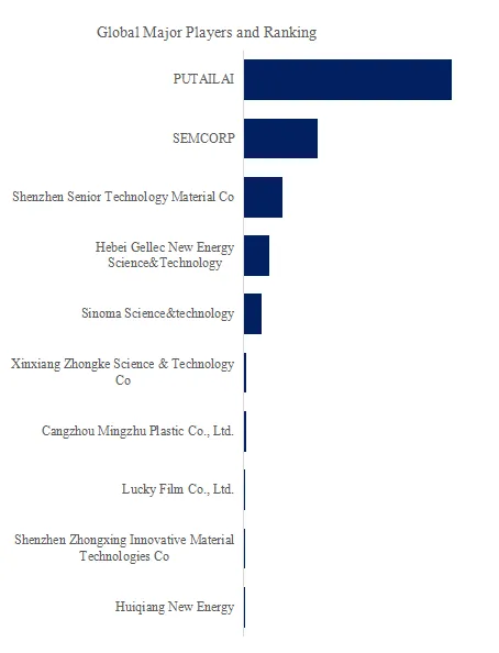
Figure00002. Global Cockpit Display System for Aerospace Top 12 Players Ranking and Market Share (Ranking is based on the revenue of 2025, continually updated)
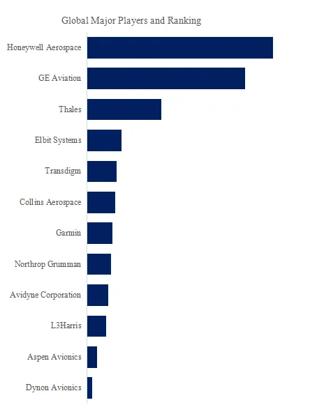
Above data is based on report from QYResearch: Global Cockpit Display System for Aerospace Market Report 2025-2031 (published in 2025). If you need the latest data, plaese contact QYResearch.
According to QYResearch Top Players Research Center, the global key manufacturers of Cockpit Display System for Aerospace include Honeywell Aerospace, GE Aviation, Thales, Elbit Systems, Transdigm, Collins Aerospace, Garmin, Northrop Grumman, Avidyne Corporation, L3Harris, etc. In 2025, the global top five players had a share approximately 66.0% in terms of revenue.
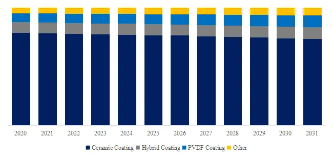
Figure00003. Cockpit Display System for Aerospace, Global Market Size, Split by Product Segment
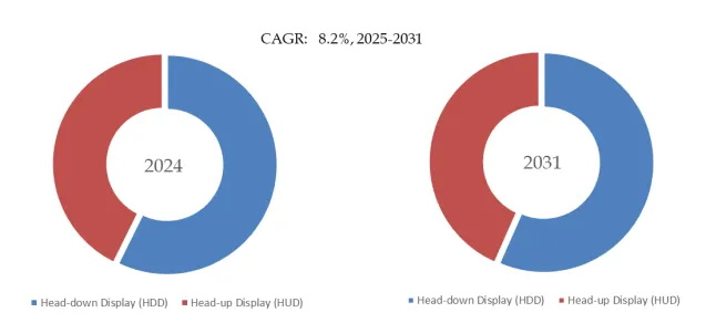
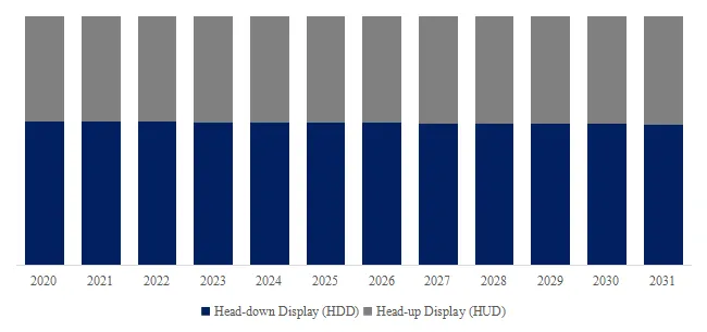
Based on or includes research from QYResearch: Global Cockpit Display System for Aerospace Market Report 2025-2031.
In terms of product type, currently Head-down Display (HDD) is the largest segment, hold a share of 57.3%.
The report provides a detailed analysis of the market size, growth potential, and key trends for each segment. Through detailed analysis, industry players can identify profit opportunities, develop strategies for specific customer segments, and allocate resources effectively.
The Cockpit Display System for Aerospace market is segmented as below:
By Company
Honeywell Aerospace
Thales
GE Aviation
Collins Aerospace
Elbit Systems
Transdigm
Northrop Grumman
Aspen Avionics
Avidyne Corporation
Garmin
L3Harris
Dynon Avionics
Segment by Type
Head-down Display (HDD)
Head-up Display (HUD)
Segment by Application
Civilian Aircraft
Military Fighter Jet
Helicopter/VSTOL
Spacecraft/Spacecraft
Each chapter of the report provides detailed information for readers to further understand the Cockpit Display System for Aerospace market:
Chapter 1: Introduces the report scope of the Cockpit Display System for Aerospace report, global total market size (valve, volume and price). This chapter also provides the market dynamics, latest developments of the market, the driving factors and restrictive factors of the market, the challenges and risks faced by manufacturers in the industry, and the analysis of relevant policies in the industry. (2021-2032)
Chapter 2: Detailed analysis of Cockpit Display System for Aerospace manufacturers competitive landscape, price, sales and revenue market share, latest development plan, merger, and acquisition information, etc. (2021-2026)
Chapter 3: Provides the analysis of various Cockpit Display System for Aerospace market segments by Type, covering the market size and development potential of each market segment, to help readers find the blue ocean market in different market segments. (2021-2032)
Chapter 4: Provides the analysis of various market segments by Application, covering the market size and development potential of each market segment, to help readers find the blue ocean market in different downstream markets.(2021-2032)
Chapter 5: Sales, revenue of Cockpit Display System for Aerospace in regional level. It provides a quantitative analysis of the market size and development potential of each region and introduces the market development, future development prospects, market space, and market size of each country in the world..(2021-2032)
Chapter 6: Sales, revenue of Cockpit Display System for Aerospace in country level. It provides sigmate data by Type, and by Application for each country/region.(2021-2032)
Chapter 7: Provides profiles of key players, introducing the basic situation of the main companies in the market in detail, including product sales, revenue, price, gross margin, product introduction, recent development, etc. (2021-2026)
Chapter 8: Analysis of industrial chain, including the upstream and downstream of the industry.
Chapter 9: Conclusion.
Benefits of purchasing QYResearch report:
Competitive Analysis: QYResearch provides in-depth Cockpit Display System for Aerospace competitive analysis, including information on key company profiles, new entrants, acquisitions, mergers, large market shear, opportunities, and challenges. These analyses provide clients with a comprehensive understanding of market conditions and competitive dynamics, enabling them to develop effective market strategies and maintain their competitive edge.
Industry Analysis: QYResearch provides Cockpit Display System for Aerospace comprehensive industry data and trend analysis, including raw material analysis, market application analysis, product type analysis, market demand analysis, market supply analysis, downstream market analysis, and supply chain analysis.
and trend analysis. These analyses help clients understand the direction of industry development and make informed business decisions.
Market Size: QYResearch provides Cockpit Display System for Aerospace market size analysis, including capacity, production, sales, production value, price, cost, and profit analysis. This data helps clients understand market size and development potential, and is an important reference for business development.
Other relevant reports of QYResearch:
Global Cockpit Display System for Aerospace Market Outlook, In‑Depth Analysis & Forecast to 2032
Global Cockpit Display System for Aerospace Market Research Report 2026
Global Cockpit Display System for Aerospace Sales Market Report, Competitive Analysis and Regional Opportunities 2026-2032
About Us:
QYResearch founded in California, USA in 2007, which is a leading global market research and consulting company. Our primary business include market research reports, custom reports, commissioned research, IPO consultancy, business plans, etc. With over 19 years of experience and a dedicated research team, we are well placed to provide useful information and data for your business, and we have established offices in 7 countries (include United States, Germany, Switzerland, Japan, Korea, China and India) and business partners in over 30 countries. We have provided industrial information services to more than 60,000 companies in over the world.
Contact Us:
If you have any queries regarding this report or if you would like further information, please contact us:
QY Research Inc.
Add: 17890 Castleton Street Suite 369 City of Industry CA 91748 United States
EN: https://www.qyresearch.com
Email: global@qyresearch.com
Tel: 001-626-842-1666(US)
JP: https://www.qyresearch.co.jp