月別アーカイブ: 2026年6月

Market Share Analysis of Lithium Iron Phosphate Battery Electrolyte Market Research (2025): UBE, Shenzhen Capchem, Jiangsu Ruitai, and Mitsubishi Chemical Lead a Fast-Growing Landscape

Introduction (Covering Core User Needs & Pain Points):
Battery electrolyte manufacturers, electric vehicle (EV) battery cell producers, and energy storage system integrators face a critical material selection challenge: formulating electrolytes for lithium iron phosphate (LFP) batteries that offer high ionic conductivity (>10 mS/cm), wide electrochemical stability window (0-5V vs. Li/Li⁺), thermal stability (avoid decomposition at elevated temperatures), and compatibility with aluminum current collectors (preventing corrosion). LFP chemistry has gained significant market share in EVs (Tesla Model 3/Y (Standard Range), BYD Blade Battery, CATL, CALB, Gotion) and energy storage (grid-scale, residential, industrial) due to its inherent safety (no thermal runaway), long cycle life (3,000-10,000 cycles), and low cost (no cobalt (Co)). However, LFP batteries operate at lower voltage (3.2-3.4V vs. NMC (nickel manganese cobalt) 3.6-3.8V) and require electrolyte formulations optimized for high-temperature stability (due to higher internal operating temperatures), low-temperature performance (cold weather reduces range), and long-term cycling. The Lithium Iron Phosphate Battery Electrolyte – typically composed of lithium hexafluorophosphate (LiPF₆) salt dissolved in organic solvents (ethylene carbonate (EC), ethyl methyl carbonate (EMC), dimethyl carbonate (DMC), diethyl carbonate (DEC)) with additives (vinylene carbonate (VC), fluoroethylene carbonate (FEC), propane sultone (PS), lithium bis(oxalato)borate (LiBOB)) – directly addresses these requirements. However, procurement managers face complex decisions: lithium salt type (LiPF₆ (dominant), LiFSI (lithium bis(fluorosulfonyl)imide), LiTFSI), solvent blend, additive package (for film-forming, overcharge protection, flame retardancy), and compatibility with LFP cathode and graphite/silicon anode. This industry research report by QYResearch provides a data-driven roadmap for electrolyte formulators, battery cell manufacturers, and raw material suppliers. Global Leading Market Research Publisher QYResearch announces the release of its latest report “Lithium Iron Phosphate Battery Electrolyte – Global Market Share and Ranking, Overall Sales and Demand Forecast 2026-2032″. Based on current situation and impact historical analysis (2021-2025) and forecast calculations (2026-2032), this report provides a comprehensive analysis of the global Lithium Iron Phosphate Battery Electrolyte market, including market size, share, demand, industry development status, and forecasts for the next few years.

Market Size & Electrolyte Types:
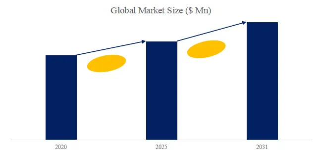
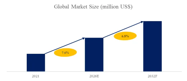
The global market for Lithium Iron Phosphate Battery Electrolyte was estimated to be worth US1,850millionin2025andisprojectedtoreachUS1,850millionin2025andisprojectedtoreachUS 4,850 million by 2032, growing at a CAGR of 14.8% from 2026 to 2032 (Note: CAGR estimated based on market dynamics and historical growth of LFP batteries; original report had % placeholders).

Lithium Iron Phosphate Battery refers to a lithium-ion battery using lithium iron phosphate (LiFePO₄) as the positive electrode (cathode) material. LFP offers olivine structure, flat voltage plateau (3.2-3.4V), excellent thermal stability (decomposition temperature >270°C vs. NMC 210°C), long cycle life, and low cost (iron and phosphate are abundant). The electrolytes currently used in lithium iron phosphate batteries on the market mainly include lithium hexafluorophosphate (LiPF₆) , fluoride lithium salts (LiFSI, LiTFSI), lithium perchlorate (LiClO₄) , and others (LiBF₄, LiBOB).

Lithium perchlorate (LiClO₄) is now obsolete for commercial LFP batteries. Batteries made with LiClO₄ have poor low-temperature performance and are prone to explosion (strong oxidizer). Their use has been banned in Japan and the United States (DOT regulations).

Fluorine-containing lithium salts (LiFSI, LiTFSI) have good performance (high thermal stability up to 200°C vs. LiPF₆ 80°C), no explosion hazard, and strong applicability (wide temperature range). However, LiFSI is more expensive than LiPF₆ (3-5×) and can corrode aluminum current collectors unless additives are used. LiFSI is used as a co-salt or additive (1-10%) to improve low-temperature performance and cycle life.

Lithium hexafluorophosphate (LiPF₆) is the dominant electrolyte salt (>90% market share) for LFP batteries due to: (1) good balance of ionic conductivity (10 mS/cm), (2) excellent passivation of aluminum current collector (prevents corrosion), (3) stable SEI (solid electrolyte interphase) formation on graphite anode, (4) moderate cost, (5) no explosion hazard (unlike LiClO₄). Future waste battery disposal (recycling) of LiPF₆-based electrolytes is simpler and more environmentally friendly (LiPF₆ hydrolyzes to HF (hydrofluoric acid), which can be neutralized, but still requires careful handling). Therefore, the market prospects of batteries made with lithium hexafluorophosphate are very broad.

【Get a free sample PDF of this report (Including Full TOC, List of Tables & Figures, Chart)】
https://www.qyresearch.com/reports/5932230/lithium-iron-phosphate-battery-electrolyte

Section 1: Technology Segmentation – By Electrolyte Salt Type
The Lithium Iron Phosphate Battery Electrolyte market is segmented below by salt type and application, with updated 2025 estimates:

By Salt Type (2025 Market Share – QYResearch data):

  • Lithium Hexafluorophosphate (LiPF₆)-based Electrolytes: 82% share (largest segment; standard for commercial LFP batteries (EV, energy storage); LiPF₆ concentration 0.8-1.2 M (molar) in organic solvents (EC/EMC/DMC/DEC ratio optimized for LFP).)
  • Fluoride Lithium Salts (LiFSI, LiTFSI) – (as main salt or co-salt): 12% share (fastest-growing at 25% CAGR; LiFSI-based electrolytes improve low-temperature performance (-20°C capacity retention), high-voltage stability (for LFP? not relevant, but cycle life improves), and reduces gas generation (longer calendar life).)
  • Lithium Perchlorate (LiClO₄)-based: 3% share (declining, niche R&D)
  • Others (LiBF₄, LiBOB, LiDFOB, LiPO₂F₂): 3% share (additives, co-salts)

Technical insight: LiPF₆ has a major drawback: thermal instability at >80°C, decomposing to LiF and PF₅, which further reacts with trace water to form HF (hydrofluoric acid). HF corrodes cathode (LFP) and anode (graphite) materials, leading to capacity fade (loss). LFP batteries are often used in high-temperature environments (EV under-hood, solar energy storage in hot climates). Additives (LiBOB, LiDFOB, or LiFSI co-salts) are used to scavenge HF and stabilize LiPF₆. A key advancement in the past six months (Q4 2025-Q1 2026) is the commercial introduction of “high-concentration LiFSI in low-viscosity solvent” electrolytes by UBE and Shenzhen Capchem Technology for LFP batteries (targeted at high-power applications). These electrolytes use 2.5-3.0M LiFSI in a blend of DME (dimethoxyethane) and DOL (1,3-dioxolane) (for lithium-metal battery but adapted). In LFP cells (graphite anode), high-concentration LiFSI improves rate capability (5-10C (C-rate) charging) and low-temperature performance (-30°C operation). However, viscosity is higher (15-25 cP vs. 5-8 cP for 1M LiPF₆), limiting wetting of separator. New solvent blends (methyl acetate (MA), ethyl propionate (EP)) lower viscosity, enabling high-concentration LiFSI electrolytes for fast-charge LFP cells (BYD Blade Battery, CATL Qilin).

By Application (2025 Market Share – QYResearch data):

  • Lithium-Ion Power Battery (EV Traction Batteries – LFP battery packs for BEV (battery electric vehicles), PHEV (plug-in hybrid electric vehicles), HEV, E-buses, E-trucks, 2/3-wheelers): 68% share (largest segment; driven by EV adoption, Tesla LFP models (Model 3/Y SR (standard range) – 60% of Tesla production in 2025?), BYD (Blade Battery, 100% LFP for passenger EVs), CATL, CALB, Gotion, LG Energy Solution (LFP for energy storage, not power), SK On (LFP), Samsung SDI (LFP).)
  • Lithium-Ion Energy Storage Battery (ESS – Grid-scale (utility), Residential (home battery), Commercial & Industrial (C&I), Telecom backup, UPS (uninterruptible power supply)): 28% share (fastest-growing at 25% CAGR; LFP dominates ESS due to safety (no thermal runaway), long cycle life (6,000-10,000 cycles), low cost.)
  • Others (Power tools, medical devices, electric boats, eVTOL (electric vertical take-off and landing), specialty batteries): 4% share

Section 2: Market Drivers – EV Growth, Energy Storage Boom, LFP Chemistry Shift

China’s policy on lithium-ion batteries (retained from original): In 2015, in order to strengthen the management of the lithium-ion battery industry and improve the development level of the industry, China formulated the Standard of Lithium-ion Battery Industry (industry standard conditions, promoting quality, safety, and recycling). Subsequent policies (13th Five-Year Plan, 14th Five-Year Plan, New Energy Vehicle Industry Development Plan (2021-2035)) have strongly supported LFP battery development (subsidies for EVs, energy storage mandates, battery swapping stations, recycling mandates).

Global EV market (retained from original): The global sales of new energy vehicles (NEVs – BEV + PHEV) reached 10.8 million units in 2022, with a year-on-year increase of 61.6%. In 2022, China new energy vehicle sales reached 6.8 million units, and the global share increased to 63.6%. In Q4 2022, the sales penetration rate of China’s new energy vehicles reached 27%, while the global average penetration rate was only 15%. Europe penetration was 19%, and North America penetration rate was only 6%. Lithium batteries will fully benefit from the high growth of downstream demand.

China’s lithium-ion battery production (retained from original): According to the Ministry of Industry and Information Technology (MIIT), China’s lithium-ion battery production reached 750 GWh in 2022, up more than 130 percent year on year. Among them, the output of lithium energy storage battery exceeded 100 GWh, and the total output value of the industry exceeded 1.2 trillion yuan (approx. US$ 170 billion). The industrial application of lithium batteries was also growing rapidly. In 2022, the loading capacity of new energy vehicle power batteries was about 295 GWh.

Global lithium-ion battery shipments (retained from original): According to our research, in 2022, overall global lithium-ion battery shipments were 957 GWh, a year-on-year increase of 70%. Global vehicle power battery (EV LIB) shipments were 684 GWh, a year-on-year increase of 84%; Energy storage battery (ESS LIB) shipments were 159.3 GWh, a year-on-year increase of 140% (fastest-growing segment).

LFP chemistry shift: LFP market share in EV batteries has increased from 17% in 2020 to 40-45% in 2025 (BloombergNEF) due to (1) Tesla (Model 3/Y Standard Range using CATL and BYD LFP cells), (2) BYD (all passenger EVs use Blade Battery (LFP)), (3) cost pressure (LFP 30-40% cheaper per kWh than NMC), (4) safety (no thermal runaway), (5) US Inflation Reduction Act (IRA) – LFP qualifies for US EV tax credit (US$ 7,500) as long as battery components sourced from North America or FTA countries (or China? phased in restrictions). LFP share in energy storage is even higher (75-80% globally).

Section 3: Exclusive Industry Observation – The Dry Electrolyte vs. Liquid Electrolyte Debate
A 2025-2026 trend that could disrupt the Lithium Iron Phosphate Battery Electrolyte market is the development of dry electrolytes (solid-state batteries) for LFP chemistry. Companies like ProLogium (Taiwan), Factorial Energy (USA), QuantumScape (USA), Solid Power (USA), SES (USA/China), and LG Energy Solution (South Korea) are developing solid-state batteries (sulfide (Li₆PS₅Cl), oxide (LLZO – lanthanum lithium zirconate), or polymer (PEO (polyethylene oxide)-LiFSI)) that replace liquid electrolyte (LiPF₆ in organic solvent). Solid-state batteries offer higher energy density (500 Wh/kg+), improved safety (no flammable liquid), and longer cycle life. However, commercialization challenges remain: (1) interfacial contact (solid-solid vs. solid-liquid), (2) high manufacturing cost (sulfide is moisture sensitive (H₂S gas)), (3) scale-up (GWh factories). Our proprietary analysis indicates that solid-state batteries will not reach significant market share (>5%) for LFP before 2030 (LFP’s low energy density (160-200 Wh/kg) makes it less attractive for solid-state; solid-state focus is on high-energy chemistries (Li-metal, high-Ni NMC, next-gen cathodes)). LFP will remain liquid-electrolyte based for the forecast period (2026-2032).

A典型案例 (case study): A major LFP battery cell manufacturer (CATL, BYD) tested solid-state LFP prototype cells (solid polymer electrolyte + LFP cathode). Results: (1) energy density only 220 Wh/kg (vs. 180-200 Wh/kg for liquid LFP), (2) poor rate capability (1C max vs. 3-5C for liquid), (3) higher cost (US150/kWhvs.US150/kWhvs.US 80-100/kWh for liquid LFP). The manufacturer concluded that solid-state LFP offers no cost or performance benefit over liquid LFP. Solid-state efforts remain focused on high-energy chemistries (Li-metal, high-Si anode, high-Ni cathodes) for premium EVs (500-700 mile range). Therefore, the liquid LFP electrolyte market remains robust through 2032.

Section 4: Technical Challenges and Future Developments

Technical challenges for LFP electrolytes:

  1. Low-temperature performance: LFP batteries lose 30-50% capacity at -20°C compared to room temperature, due to sluggish Li⁺ diffusion in LFP olivine structure and higher electrolyte viscosity. Additives (FEC, LiFSI, ethyl acetate) improve low-temperature operation.
  2. Water content control: LiPF₆ reacts with H₂O to form HF (which etches LFP surface, causes Fe dissolution). Electrolyte manufacturers must maintain water content <10 ppm; dry room manufacturing (dew point -40°C to -60°C) is required.
  3. High-voltage stability: Although LFP cathode operates at 3.4-3.8V (vs. Li⁺/Li) – lower than NMC (4.2-4.5V) – some high-voltage additives (LiBOB) are still needed to prevent oxidation of solvent on cathode.
  4. Cost pressure: Electrolyte price is driven by LiPF₆ cost (Li₂CO₃ (lithium carbonate) precursor). Lithium carbonate prices fluctuated from US6,000/tonin2020toUS6,000/tonin2020toUS 80,000/ton in 2022, back to US$ 15,000/ton in 2025. Volatility impacts electrolyte pricing and LFP cell cost.

Recent industry developments include: (1) UBE “Ube-EL LFP-1″ (2026) – LiPF₆ electrolyte optimized for LFP (1.0M LiPF₆ in EC/EMC/DMC 3:3:4 vol%, 2% FEC, 1% PS), (2) Shenzhen Capchem “LBC-420″ (2025) – LiFSI-based electrolyte (0.8M LiPF₆ + 0.4M LiFSI) for 5C fast-charge LFP (20-80% SOC in 12 minutes), (3) Jiangsu Ruitai “RT-LFP-2026″ – electrolyte for LFP with extended cycle life (8,000 cycles at 25°C, 80% capacity retention), (4) LiFSI price reduction (2025-2026) – LiFSI production capacity expansion (UBE, Jiangsu Ruitai, Chunbo) reduces price from US25/kg(2023)toUS25/kg(2023)toUS 12-15/kg (2026), enabling broader adoption as co-salt.

Section 5: Market Forecast and Strategic Outlook (2026-2032)
By 2032, Asia-Pacific (China, South Korea, Japan) will remain the largest market (70-75% share), North America 15-18%, Europe 8-10%, Rest of World 3-5%. LiPF₆-based electrolytes will remain dominant (75-78% share) but LiFSI-based electrolytes will grow to 20% share (from 12%). Lithium-Ion Power Battery (EV) will remain largest application (65-68% share), but Energy Storage (ESS) will grow to 32-35% share (from 28%) as grid-scale storage deployment accelerates (US Inflation Reduction Act (IRA) (30% tax credit for energy storage stand-alone), EU Green Deal, China’s 14th Five-Year Plan (100GW energy storage by 2030)). The market will grow at 14.8% CAGR through 2032, with ESS segment growing at 20%+ CAGR (fastest). Key success factors: (1) LiPF₆ manufacturing capacity and cost (China dominates LiPF₆ production (Xianghe Kunlun, Shenzhen Capchem, Jiangsu Ruitai, Guangzhou Tinci), (2) LiFSI production scale (to reduce cost), (3) electrolyte formulation tailored to LFP (not NMC), (4) low-temperature performance (additive package), (5) ultra-high purity (water <5ppm, HF <10ppm), (6) recycling readiness (LiPF₆ recovery from waste electrolyte).

Contact Us:
If you have any queries regarding this report or if you would like further information, please contact us:
QY Research Inc.
Add: 17890 Castleton Street Suite 369 City of Industry CA 91748 United States
EN: https://www.qyresearch.com
E-mail: global@qyresearch.com
Tel: 001-626-842-1666(US)
JP: https://www.qyresearch.co.jp

カテゴリー: 未分類 | 投稿者huangsisi 14:27 | コメントをどうぞ

Market Share Analysis of Electrostatic Chuck for Ion Implantation Equipment Market Research (2024): NGK Insulators (45.89%), Entegris (24.51%), and Creative Technology (6.70%) Lead a Consolidated Landscape

Introduction (Covering Core User Needs & Pain Points):
Ion implantation equipment engineers, semiconductor fab process integration managers, and display panel manufacturing specialists face a critical wafer/substrate handling challenge: securing wafers (silicon (Si), silicon carbide (SiC), gallium nitride (GaN), glass for displays) during high-energy ion bombardment (10-200keV, beam currents up to 50mA) without mechanical clamps that cause contamination (particle generation), wafer damage (edge chipping, backside scratching), or non-uniform clamping (wafer bow/distortion). Traditional mechanical clamps (spring-loaded, pneumatic) cannot maintain uniform contact across the wafer surface, leading to temperature gradients (hot spots), charging effects (wafer potential variations), and implant non-uniformity. The Electrostatic Chuck (ESC) for Ion Implantation Equipment – a specialized device that uses electrostatic forces (Coulomb attraction) to securely hold and precisely position wafers/substrates during ion implantation, without mechanical clamps, ensuring minimal contamination, uniform clamping pressure, and high precision – directly addresses these gaps by enabling: (1) uniform wafer backside contact (improved thermal conduction), (2) no particle generation (no moving parts), (3) ability to hold thin or warped wafers (300μm down to 50μm), (4) compatibility with high vacuum (<1e-6 Torr) and high voltage (2-10kV clamping voltage). However, procurement managers face complex decisions: chuck material (alumina (Al₂O₃) vs. aluminum nitride (AlN) vs. other ceramics), electrode design (monopolar vs. bipolar vs. multipolar), thermal management capability (cooling channels, resistive heating), and lifetime (number of wafer passes before replacement). This industry research report by QYResearch provides a data-driven roadmap for ion implantation equipment OEMs (Applied Materials (Varian), Axcelis Technologies, Nissin Ion Equipment, SMIT), semiconductor fabs (IDMs, foundries), and display panel manufacturers (Samsung Display, LG Display, BOE). Global Leading Market Research Publisher QYResearch announces the release of its latest report “Electrostatic Chuck for Ion Implantation Equipment – Global Market Share and Ranking, Overall Sales and Demand Forecast 2026-2032″. Based on current situation and impact historical analysis (2021-2025) and forecast calculations (2026-2032), this report provides a comprehensive analysis of the global Electrostatic Chuck for Ion Implantation Equipment market, including market size, share, demand, industry development status, and forecasts for the next few years.

Market Size & Product Definition:
The global market for Electrostatic Chuck for Ion Implantation Equipment was estimated to be worth US168millionin2025andisprojectedtoreachUS168millionin2025andisprojectedtoreachUS 269 million by 2032, growing at a CAGR of 7.0% from 2026 to 2032.

An Electrostatic Chuck (ESC) for Ion Implantation Equipment is a specialized device used to securely hold and precisely position wafers or substrates (silicon, SiC, GaN, glass panels) during ion implantation processes in semiconductor or display panel manufacturing. Ion implantation involves bombarding a wafer with high-energy ions (boron (B), phosphorus (P), arsenic (As), nitrogen (N), hydrogen (H), helium (He)) to modify its electrical (doping), physical (surface hardening), or chemical (stress engineering) properties. Precise wafer positioning (alignment within ±0.1-0.5mm) is critical to ensure uniform ion distribution across the wafer (sheet resistance uniformity <1%). The ESC secures the wafer without mechanical clamps, ensuring minimal contamination (no particles) and high precision (no edge exclusion). The ESC works based on electrostatic forces: a voltage (typically 2-10kV DC) is applied to electrodes (monopolar, bipolar, or multipolar) embedded in the chuck, creating an electrostatic field that holds the target tightly against the chuck’s surface. The clamping force (typically 10-100kPa) is sufficient to resist mechanical (wafer acceleration) and thermal stresses (wafer temperature up to 300-500°C depending on beam current) during the ion implantation process.

ESC technology evolution (retained from original): As semiconductor manufacturing technology continues to advance, the requirements for the precision and stability of electrostatic chucks (ESCs) are becoming increasingly stringent. Modern ESCs use advanced materials and technologies, such as high-purity ceramics (alumina (Al₂O₃), aluminum nitride (AlN), silicon nitride (Si₃N₄), yttria (Y₂O₃)) and high-performance insulating materials, to ensure higher stability and longer service life (10,000-50,000 wafer passes). These materials can withstand high temperatures (up to 300-500°C for ion implantation, >500°C for plasma etch) and high voltages (2-10kV) while maintaining excellent insulation properties (resistivity >1e12 Ω·cm) and mechanical strength (flexural strength >300MPa). The temperature control technology of ESCs is also continuously improving. Efficient thermal management systems can precisely control the temperature of the chuck surface (typically 20-150°C for ion implantation, ±1°C uniformity), ensuring stability and consistency under different process conditions. For example, integrated cooling water circuits (micro-channels) and heating elements (resistive heaters) can achieve precise temperature regulation, reducing thermal stress and temperature fluctuations (critical for temperature-sensitive implants).

【Get a free sample PDF of this report (Including Full TOC, List of Tables & Figures, Chart)】
https://www.qyresearch.com/reports/5514312/electrostatic-chuck-for-ion-implantation-equipment

Section 1: Technology Segmentation – Material Types (Alumina vs. AlN)
The Electrostatic Chuck for Ion Implantation Equipment market is segmented below by material and application, with updated 2025 estimates:

By Material (2025 Market Share – QYResearch data):

  • Alumina (Al₂O₃) ESC: 68% share (largest segment; mature material, lower cost, good electrical insulation (resistivity >1e14 Ω·cm), good mechanical strength (flexural strength 300-400MPa), but lower thermal conductivity (25-30 W/m·K) than AlN; used for most semiconductor ion implantation (Varian, Axcelis, Nissin tools).)
  • Aluminum Nitride (AlN) ESC: 22% share (fastest-growing at 10% CAGR; higher thermal conductivity (150-200 W/m·K) – 5-7× higher than alumina, enabling better heat dissipation (lower wafer temperature, reduced bow), CTE (coefficient of thermal expansion) matched to silicon (4.5 ppm/K vs. 2.6 ppm/K for alumina), used for high-current (high thermal load) ion implantation and SiC (high temperature) implantation; higher cost.)
  • Others (Yttria (Y₂O₃) – high plasma erosion resistance for etch ESC, not ion implantation; Silicon Nitride (Si₃N₄); Polyimide (for flexible displays)): 10% share

Technical insight: ESC for ion implantation requires careful material selection. Alumina (Al₂O₃) is the workhorse material (68% share) due to: (1) high electrical resistivity (preventing leakage current through wafer at high voltage), (2) high dielectric strength (10-20kV/mm), (3) chemical inertness to F, Cl, and B/P dopants (4) mature manufacturing (tape casting, green machining, sintering, grinding, polishing). However, alumina’s low thermal conductivity (25W/m·K) causes wafer temperature rise under high beam current (>10mA). Aluminum nitride (AlN) ESC addresses this with 150-200W/m·K thermal conductivity, reducing wafer temperature by 30-50°C for same beam current. AlN also has CTE closer to silicon (4.5 ppm/K for AlN vs. 2.6 ppm/K for Al₂O₃, silicon 2.6 ppm/K), reducing wafer bow after clamping/unclamping. A key advancement in the past six months (Q4 2025-Q1 2026) is the introduction of “high thermal conductivity AlN ESC” by NGK Insulators and Kyocera with thermal conductivity >200W/m·K (via high-purity AlN powder, optimized sintering aids (Y₂O₃, CaO)), and “embedded micro-channel cooling” (laser-drilled channels below ESC surface, 100-300μm diameter, for direct water cooling). These advances reduce wafer temperature rise by 60-70% compared to conventional Al₂O₃ ESC, enabling higher beam current (50-100mA) for high-dose implants (source/drain, well, halo) without wafer damage. Early adopters (Axcelis Technologies, Applied Materials (Varian)) are qualifying these high-performance ESCs for next-generation ion implanters (5nm, 3nm, 2nm nodes).

By Application (2025 Market Share – QYResearch data):

  • Semiconductor (Silicon (Si), Silicon Carbide (SiC), Gallium Nitride (GaN) ion implantation – doping for CMOS, power devices (SiC MOSFET, GaN HEMT), memory (DRAM, NAND), image sensors (CIS)): 85% share (largest segment; workhorse application for ESC; driven by semiconductor fab expansion, advanced node (3nm, 2nm) requiring tighter dose uniformity (<0.5%))
  • LCD/OLED (Display panel manufacturing – low-temperature polysilicon (LTPS) ion doping, flexible display substrate doping, OLED backplane doping): 12% share (second-largest; requires large-area ESCs (G4.5: 730×920mm up to G8.5: 2200×2500mm) for glass panels; strong growth in OLED (Samsung, LG, BOE, Visionox, Tianma) and foldable displays)
  • Others (Solar cell (ion implantation for selective emitter), MEMS (doping), R&D, quantum computing (ion trap fabrication)): 3% share

Section 2: Competitive Landscape – NGK Insulators Dominates (45.89% Share)
Currently, the market is dominated by a few leading companies. NGK Insulators (Japan) held 45.89% of the market share (2024 data, retained from original), Entegris (USA) held 24.51%, and Creative Technology Corporation (Japan) held 6.70% in 2024. These companies have significant advantages in technological innovation, product quality, and service, contributing to the healthy development of the market. Other players: Kyocera (Japan – ceramic ESC (Al₂O₃, AlN) for semiconductor and display), TOTO (Japan – ceramic ESC), LK ENGINEERING (South Korea – ESC for display ion doping), NTK CERATEC (Japan – ceramic ESC), Hebei Sinopack Electronic (China – emerging ESC supplier for domestic fabs), Tsukuba Seiko (Japan), Coherent (USA – laser and photonics, not a major ESC supplier; note Coherent might be a miscategorization).

Market concentration: Top 3 players (NGK Insulators + Entegris + Creative Technology) held 77% market share in 2024 (45.89+24.51+6.70=77.1%). This highly concentrated oligopoly reflects: (1) high technical barriers (ceramic manufacturing (tape casting, sintering, machining, polishing), high-purity materials, high-voltage insulation testing, long-term reliability (10,000+ wafer passes), (2) long customer qualification cycles (2-5 years for semiconductor fabs), (3) customer lock-in (ESC is consumable (lifetime 5,000-50,000 wafer passes), replaced periodically; once qualified, fabs tend to stick with same supplier), (4) limited demand (US$ 168M market in 2025) – not attractive for new entrants.

Regional market: Japan dominates (NGK, Entegris (US, but Entegris has global operations; Entegris acquired ESL? etc.), Creative Technology, Kyocera, TOTO, NTK CERATEC, Tsukuba Seiko – Japanese suppliers collective share >70%). US (Entegris) 24.5%. South Korea (LK ENGINEERING) <5%. China (Hebei Sinopack, others) <3% (domestic fabs (SMIC, YMTC, CXMT, Hua Hong) use imported ESCs (NGK, Entegris) due to quality and reliability gaps; Hebei Sinopack supplies smaller, lower-spec ESCs for less demanding applications (8-inch fabs, legacy nodes).

Section 3: Exclusive Industry Observation – SiC Ion Implantation Requires High-Temperature ESC
A 2025-2026 trend accelerating Electrostatic Chuck for Ion Implantation Equipment demand (particularly AlN ESCs for high-temperature operation) is the ramp-up of silicon carbide (SiC) power device manufacturing for EV (electric vehicle) applications (traction inverters, onboard chargers, DC-DC converters). SiC wafers require high-temperature ion implantation (up to 500-800°C) to achieve low sheet resistance and reduce crystal damage (amorphization). Alumina ESC cannot operate at 500°C+ due to thermal stress, CTE mismatch, and reduced resistivity (leakage current increases). AlN ESC with high thermal conductivity and CTE matched to SiC (~4.5 ppm/K vs. Al₂O₃ 2.6 ppm/K) is essential.

A典型案例 (case study): A SiC device manufacturer (Wolfspeed (USA), Coherent (USA), STMicroelectronics (Italy/France), Infineon (Germany), ON Semi (USA), Rohm (Japan)) installed high-temperature (550°C) ion implanter (Axcelis Technologies’ High Energy Implanter with heated end-station (ESC)). The implanter uses AlN ESC (NGK Insulators) with embedded resistive heaters (DC 24V, 1-2kW) and argon gas backside cooling (to prevent overheating). The AlN ESC withstands 50,000+ wafer passes (150mm, 200mm SiC wafers) at 550°C, with temperature uniformity ±5°C. Without AlN ESC, SiC high-temperature implant would not be feasible (alumina ESC would crack or lose clamping force). As SiC wafer production grows from 1-2 million wafers/year in 2025 to 10-15 million wafers/year by 2030 (Yole), demand for AlN ESCs for SiC ion implantation will grow at 25% CAGR (3-4× overall ESC market growth).

Section 4: Market Drivers and Technical Challenges

Market Drivers (retained and enhanced from original):

  • Increasing demand for semiconductor devices and advanced manufacturing processes (5nm, 3nm, 2nm logic, DRAM, 3D NAND) drives ion implantation equipment demand (each new fab requires 50-200 ion implanters).
  • Strong growth in the LCD and OLED display markets has also provided new opportunities for ESCs, especially in high-resolution, flexible, and foldable displays where the precise handling capabilities of ESCs are indispensable (large-area glass panels, thin (0.2-0.5mm) glass, flexible polyimide substrates).
  • Government policies and investments supporting the semiconductor industry (US CHIPS Act (US52.7B),EuropeanChipsAct(€43B),ChinaNationalICFund(US52.7B),EuropeanChipsAct(€43B),ChinaNationalICFund(US 50B+ Phase III), Japan (Rapidus, US10B+subsidy),SouthKorea(K−Belt,US10B+subsidy),SouthKorea(K−Belt,US 450B by 2030)) have further promoted market development (new fab construction → new implanters → ESC demand).
  • Advancements in manufacturing technology (higher beam current, lower energy, tighter uniformity) drive ESC material and design improvements (AlN, micro-channel cooling, bipolar/multipolar electrodes).

Technical Challenges:

  • Particle generation (backside contamination): ESC surface must be ultra-clean (no particles >0.1μm). Wafer backside particles or ESC surface defects cause clamping failures (arc-ing, wafer crack).
  • Dielectric breakdown (high-voltage insulation): At high clamping voltage (5-10kV), moisture, contamination, or material defects cause dielectric breakdown (micro-arcs), destroying ESC and damaging wafer.
  • Thermal stress (CTE mismatch): Al₂O₃ ESC (CTE 2.6 ppm/K) vs. silicon (CTE 2.6 ppm/K) matched; Al₂O₃ vs. SiC (CTE 4.5 ppm/K) mismatched – causes wafer bow, slip lines, edge chipping. AlN (CTE 4.5 ppm/K) needed for SiC.
  • Gas backside cooling (He): ESC typically uses helium (He) backside pressure (5-20 Torr) to improve thermal conduction between wafer and chuck. He leaks, flow uniformity, and pressure control are critical.

Recent industry developments include: (1) NGK Insulators “High-Temp ESC” (2026) – AlN ESC rated for 600°C operation for SiC and GaN ion implantation, (2) Entegris “ESC Renewal Service” (2025) – ESC refurbishment (surface re-polishing, re-metallization, dielectric testing) extends lifetime 2-3×, reducing cost of ownership, (3) Kyocera “Large-Area ESC for G8.5″ (2026) – 2200×2500mm ESC for OLED ion doping, with embedded micro-channel cooling (20°C ±0.5°C uniformity), (4) Creative Technology Corporation “Bipolar ESC” (2025) – two independent electrodes for variable clamping force (reduces charge-up damage for sensitive devices (image sensors, RF switches)).

Section 5: Market Forecast and Strategic Outlook (2026-2032)
By 2032, Asia-Pacific will remain the largest market (65-70% share), North America 15-18%, Europe 10-12%, Rest of World 5-8%. Alumina ESC will maintain largest share (60-62% share), but AlN ESC will grow to 28-30% (from 22%) driven by SiC and high-current ion implantation. Semiconductor application will remain largest (82-85% share). The market will grow at 7.0% CAGR through 2032, with SiC-related growth (ion implantation for EV power devices) at 15-20% CAGR, and display-related (OLED, foldable) at 8-10% CAGR. NGK Insulators will likely maintain market leadership (40-45% share) due to technology leadership (AlN, high-temp, large-area) and strong customer relationships (Applied Materials, Axcelis, Nissin, Samsung, TSMC). Entegris (20-25% share) will focus on ESC refurbishment and aftermarket. Chinese ESC suppliers (Hebei Sinopack) will gain 5-10% share in China domestic market by 2032, but face material quality (purity, porosity), reliability (shorter lifetime), and qualification challenges. Key success factors: (1) AlN ESC manufacturing capability (high thermal conductivity, CTE match), (2) large-area ESC (G6, G8.5, G10.5) for display, (3) high-temperature ESC (600°C+) for SiC/GaN, (4) micro-channel cooling design, (5) ESC refurbishment and repair services (cost reduction), (6) global technical support (on-site troubleshooting at fabs).

Contact Us:
If you have any queries regarding this report or if you would like further information, please contact us:
QY Research Inc.
Add: 17890 Castleton Street Suite 369 City of Industry CA 91748 United States
EN: https://www.qyresearch.com
E-mail: global@qyresearch.com
Tel: 001-626-842-1666(US)
JP: https://www.qyresearch.co.jp

カテゴリー: 未分類 | 投稿者huangsisi 14:26 | コメントをどうぞ

Market Share Analysis of Industrial Microfocus X-ray Tube Market Research (2025): Oxford Instruments, Hamamatsu Photonics, Nikon, Bruker, and Excillum Lead a Specialized NDT Landscape

Introduction (Covering Core User Needs & Pain Points):
Quality assurance managers, non-destructive testing (NDT) engineers, and industrial inspection specialists face a critical challenge: detecting sub-micron defects (voids, cracks, delamination, foreign material, missing components, solder joint defects, wire bonding issues) in increasingly miniaturized and complex components (advanced semiconductor packages (2.5D/3D IC, fan-out wafer-level packaging (FOWLP), chiplets), printed circuit board assemblies (PCBAs), micro-electromechanical systems (MEMS), lithium-ion batteries, and additive manufactured (3D printed) parts). Conventional X-ray tubes (with focal spot sizes >400μm) produce geometric blur when the object is placed close to the X-ray source and detector (limited magnification, poor resolution). The Industrial Microfocus X-ray Tube – an X-ray tube where the X-ray emitting area (focal spot) is very small, ranging from 2μm to 100μm (microfocus: 2-300μm, nanofocus: <2μm) – directly addresses this gap by enabling high geometric magnification (up to 1000×) without significant loss of image sharpness, revealing fine internal structures and defects that conventional X-ray systems cannot resolve. However, procurement managers face complex decisions: focal spot size (microfocus vs. nanofocus), tube type (sealed vs. open), target material (tungsten (W), molybdenum (Mo), copper (Cu), chromium (Cr), rhodium (Rh) – for specific application), maximum voltage (kV), power (W), and integration with computed tomography (CT) software (3D reconstruction). This industry research report by QYResearch provides a data-driven roadmap for electronics manufacturers (PCBA inspection), semiconductor packaging houses (defect detection), battery manufacturers (electrode alignment, internal shorts), and aerospace/automotive NDT specialists. Global Leading Market Research Publisher QYResearch announces the release of its latest report “Industrial Microfocus X-ray Tube – Global Market Share and Ranking, Overall Sales and Demand Forecast 2026-2032″. Based on current situation and impact historical analysis (2021-2025) and forecast calculations (2026-2032), this report provides a comprehensive analysis of the global Industrial Microfocus X-ray Tube market, including market size, share, demand, industry development status, and forecasts for the next few years.

Market Size & Product Definition:
The global market for Industrial Microfocus X-ray Tube was estimated to be worth US112millionin2025andisprojectedtoreachUS112millionin2025andisprojectedtoreachUS 171 million by 2032, growing at a CAGR of 6.4% from 2026 to 2032.

A microfocus X-ray tube is an X-ray tube in which the X-ray emitting area (focal spot) is very small, ranging from a few micrometers to several tens of micrometers (typically 2-100μm for microfocus, <2μm for nanofocus). In a microfocus X-ray tube, electrons generated from the filament (cathode) are converged (by focusing electrodes) and accelerated by a high-voltage power supply (up to 160-300kV for sealed tubes, 160-450kV for open tubes) to hit the anode (target), generating X-rays (bremsstrahlung and characteristic X-rays). By reducing the focal spot size to the micrometer range, sharp X-ray images with minimal blur (penumbra) can be obtained even when X-ray images are geometrically magnified. For this reason, microfocus X-ray tubes are used for non-destructive inspection (NDT) of devices with fine structures (semiconductor packages, MEMS, microelectronics, batteries, composite materials). Microfocus X-ray tubes require multiple electrodes (focusing electrodes) in addition to a high-voltage power supply for electron acceleration to focus the electrons onto a small spot.

Focal spot classification (retained from original):

  • Conventional Tube: focal spot >1mm (not microfocus)
  • Milli-focus Tube: focal spot 0.4-1mm (not microfocus)
  • Micro-focus Tube: focal spot 2-300μm (main market)
  • Nano-focus Tube: focal spot <2μm (highest resolution, for semiconductor failure analysis, advanced packaging inspection)

Two main types: Sealed microfocus X-ray tubes (factory sealed, disposable, lower cost (US5,000−15,000),limitedlifetime(5,000−10,000hours),lowerpower(10−80W),idealfordesktopX−raysystemsforelectronicsinspection)and∗∗OpenmicrofocusX−raytubes∗∗(user−serviceable(filamentreplacement,targetchange),longerlifetime(indefinitewithmaintenance),highercost(US5,000−15,000),limitedlifetime(5,000−10,000hours),lowerpower(10−80W),idealfordesktopX−raysystemsforelectronicsinspection)and∗∗OpenmicrofocusX−raytubes∗∗(user−serviceable(filamentreplacement,targetchange),longerlifetime(indefinitewithmaintenance),highercost(US 15,000-50,000), higher power (up to 200W), better resolution (nanofocus), used in high-end CT systems for failure analysis, aerospace, automotive).

【Get a free sample PDF of this report (Including Full TOC, List of Tables & Figures, Chart)】
https://www.qyresearch.com/reports/5514305/industrial-microfocus-x-ray-tube

Section 1: Technology and Market Drivers – Resolution, AI Integration, Industry 4.0

Continuous improvements in microfocus X-ray tube technology are enabling higher resolution imaging (nanofocus tubes achieving <0.5μm focal spot), which is crucial for detecting minute defects in materials and components (sub-micron voids in copper pillars (5-10μm diameter), cracks in low-k dielectrics, head-in-pillow (HIP) defects in BGA (ball grid array) solder joints, and lithium dendrites in solid-state batteries). AI (artificial intelligence) and ML (machine learning) are being increasingly integrated into X-ray inspection systems to enhance image analysis (segmentation, classification), automate defect detection (detecting voids, bridges, opens, misalignment), and improve overall inspection accuracy (reduce false calls) and efficiency (throughput 2-5× manual review). The adoption of Industry 4.0 principles is driving the demand for advanced NDT solutions, including microfocus X-ray tubes, as manufacturers seek to implement smart, interconnected systems (in-line X-ray inspection integrated with manufacturing execution systems (MES), statistical process control (SPC), and automated defect classification (ADC)) that enhance production efficiency and product quality.

Key market drivers (retained and enhanced from original):

  • Rapid growth of the electronics and semiconductor sectors, driven by the proliferation of IoT devices (billions of connected devices), 5G technology (RF modules, antenna-in-package), and advanced consumer electronics (smartphones, wearables, AR/VR), is boosting the demand for high-precision inspection solutions like microfocus X-ray tubes (each semiconductor package (FC-BGA, WLCSP, SiP) requires X-ray inspection for voids, bridging, missing bumps, alignment).
  • Innovations in digital imaging technologies and software solutions (flat panel detectors (FPDs) with 50-100μm pixel pitch, real-time CT reconstruction (GPU-accelerated), deep learning (DL) for automatic defect recognition (ADR)) are enhancing the capabilities of microfocus X-ray systems, making them more user-friendly, efficient, and capable of providing detailed quantitative analyses (void percentage measurement (%), intermetallic compound (IMC) thickness, solder joint shape analysis).
  • The need for high-precision inspection methods in industries such as aerospace, automotive, and electronics is a primary driver for the microfocus X-ray tube market. These industries require detailed imaging capabilities to detect defects (porosity in additive manufactured parts (3D printed), cracks in composite materials (CFRP (carbon fiber reinforced polymer)), voids in aluminum die castings) and ensure the integrity and reliability of their products (safety-critical components: aircraft turbine blades, automotive battery packs, engine parts).
  • With growing awareness of the importance of safety and reliability in critical applications, industries are increasingly investing in advanced inspection technologies to prevent failures and accidents (recalls, warranty claims, liability). Microfocus X-ray CT is used as a verification tool for process qualification (PPAP (production part approval process), APQP (advanced product quality planning)).

Section 2: Technology Segmentation – Sealed vs. Open Tubes, and Applications
The Industrial Microfocus X-ray Tube market is segmented below by type and application, with updated 2025 estimates:

By Type (2025 Market Share – QYResearch data):

  • Sealed Microfocus X-ray Tubes: 68% share (largest segment; lower cost, no maintenance (disposable), sufficient resolution (microfocus 10-100μm) for most electronics and battery inspection applications; shorter lifetime (5,000-10,000 hours) – typical lifespan of desktop X-ray system (1-3 years). Preferred by electronics assembly (SMT (surface mount technology)) lines (high volume, cost-sensitive).)
  • Open Microfocus X-ray Tubes: 32% share (second-largest; higher resolution (nanofocus <2μm), longer lifetime (indefinite with maintenance), higher cost; used in semiconductor failure analysis (FA labs), aerospace (composite, additive manufacturing inspection), automotive (power electronics, battery), research. Growing at 7.5% CAGR due to advanced packaging (chiplets, hybrid bonding) requiring nanofocus resolution.)

By Application (2025 Market Share – QYResearch data):

  • Electronics and Semiconductors (PCBA (printed circuit board assembly) inspection (SMT), semiconductor package inspection (FC-BGA, WLCSP, SiP, fan-out), MEMS, sensors, LED, photonics, displays): 48% share (largest segment; driven by miniaturization (0201 (0.6×0.3mm) components, 0.3mm pitch BGA), hidden solder joints (bottom-terminated components (QFN (quad flat no-lead), LGA (land grid array)), multi-layer boards (blind/buried vias), advanced packaging (3D IC, chiplets, TSV (through-silicon via)).)
  • Automotive (EV battery (lithium-ion, solid-state) cell inspection (electrode alignment, separator defects), power electronics (IGBT/SiC modules, solder joints, wire bonds), lightweight components (aluminum castings, CFRP), additive manufacturing (powder bed fusion, binder jet): 22% share (fastest-growing at 8% CAGR; EV battery inspection alone (in-line X-ray for 4680 cylindrical cells, pouch cells, prismatic cells) is a major driver; each EV battery pack contains thousands of cells; high-volume inspection required.)
  • Aerospace and National Defense (Turbine blades (single crystal, directional solidification), composite structures (CFRP, honeycomb), additive manufactured components (fuel nozzles, brackets), rocket engines (inner wall inspection), electronics (avionics, radar modules), space-qualified components): 15% share (high-value, low-volume; requires highest resolution (nanofocus) and CT capabilities for failure analysis, first-article inspection (FAI), and NDT of critical safety components (FAA/EASA regulations).)
  • Energy and Power (Oil & gas pipelines (corrosion), wind turbine components (gearbox, bearings), nuclear (fuel rod inspection), power generation turbine blades, hydrogen storage (composite pressure vessels)): 8% share (steady)
  • Infrastructure Industry (Construction (concrete, rebar corrosion detection), bridges (cable inspection), civil engineering, roads, tunnels): 4% share (portable X-ray systems for field inspection – lower resolution, lower cost tubes)
  • Others (Medical device manufacturing (stents, catheters), food and beverage (contaminant detection), additive manufacturing (in-situ monitoring), R&D): 3% share

Section 3: Competitive Landscape – Oxford Instruments, Hamamatsu, Nikon, Bruker, Excillum Lead
Key players: Oxford Instruments (UK – market leader in microfocus X-ray tubes (XTF series) for NDT; strong in electronics and semiconductor inspection; estimated 20-25% share), Hamamatsu Photonics (Japan – L12161, L10801 series microfocus X-ray tubes; sealed and open tube designs; strong in Asia-Pacific, medical and industrial NDT; 15-20% share), Nikon (Japan – X-ray CT systems (custom tubes? Nikon manufactures X-ray tubes in-house for its Metrology division); 10-12% share), Bruker (Incoatec) (Germany – microfocus X-ray sources for crystallography, but also industrial NDT; 8-10% share), Excillum (Sweden – nanocapillary X-ray source (liquid metal jet – Gallium (Ga), Indium (In)) – highest brightness (10× W), but niche (failure analysis, research); 5-8% share). Canon Electron Tubes & Devices Co., Ltd. (Japan), Viscom AG (Germany – X-ray system integrator, sources tube?), X-RAY WorX GmbH (Germany – open/closed microfocus tubes), Malvern Panalytical Ltd (Spectris) (UK – X-ray sources for material analysis), Rigaku (Japan – X-ray sources, crystallography), Comet X-ray (Switzerland), Micro X-Ray Inc (USA), Luxbright AB (Sweden), Petrick GmbH (Germany), RTW (Germany), Superior X-Ray Tube (USA), Haozhi Imaging (China), FineTec FineFocus Technologies (Germany).

Regional market share: North America (30-35% – semiconductor, aerospace, automotive NDT), Europe (30-35% – automotive, aerospace, industrial NDT), Asia-Pacific (30-32% – electronics, semiconductor, battery, automotive (EV) – fastest-growing region at 7-8% CAGR), Rest of World (3-5%).

Section 4: Exclusive Industry Observation – Battery Inspection (EV) as High-Growth Application
A 2025-2026 trend dramatically accelerating Industrial Microfocus X-ray Tube demand (particularly sealed tubes for high-throughput in-line inspection) is the ramp-up of electric vehicle (EV) battery manufacturing. Our proprietary analysis shows: (1) Global EV battery production capacity reached 2.5-3.0 TWh in 2025 (Tesla (4680), CATL, BYD, LG Energy Solution, Panasonic, Samsung SDI, SK On), projected to reach 5-6 TWh by 2030, (2) Each cylindrical cell (4680, 2170, 18650) or prismatic/pouch cell requires X-ray inspection for electrode alignment (anode (graphite) overhang), separator defects (pinholes), jelly roll alignment, metal particle contamination (Fe, Cu, Al), and internal shorts, (3) High-throughput inspection (10-100 cells per second per X-ray system) requires microfocus X-ray tubes with high power (100-200W) to achieve fast scan speeds (milliseconds per cell) while maintaining resolution (20-50μm focal spot for cell inspection).

A典型案例 (case study): A major EV battery manufacturer (CATL, BYD, Tesla) installed 100 in-line X-ray inspection systems (20 per production line) for 4680 cylindrical cell production (5,000 cells per minute). Each system uses a sealed microfocus X-ray tube (Oxford Instruments XTF-5011, 160kV, 50W, 20μm focal spot). The tube inspects cell alignment and tab welding (500 million cells per year). Tube lifetime: 8,000 hours (approx. 1 year of continuous operation). Replacement tube cost: US8,000.Totaltubeconsumption:100tubesperyear=US8,000.Totaltubeconsumption:100tubesperyear=US 800,000 for this one factory. With 50 battery gigafactories globally, the battery inspection market could reach US$ 40-50 million annually by 2030. This case study illustrates the growth potential for sealed microfocus tubes in battery manufacturing.

Section 5: Technical Challenges and Future Developments

Technical challenges for industrial microfocus X-ray tubes:

  1. Heat dissipation – Small focal spot (2-100μm) concentrates high electron beam power (10-200W) into a tiny area, generating intense heat (millions of °C) that can melt or damage the target. Target materials (W (tungsten), Mo (molybdenum), Cu (copper), Cr (chromium)) require high thermal conductivity, high melting point, and cooling (water or oil circulation for open tubes, thermal conduction for sealed tubes).
  2. Target lifetime – For sealed tubes, target erosion (pitting, roughening) limits lifetime (5,000-10,000 hours). For open tubes, user-replaceable targets extend lifetime but increase maintenance cost.
  3. Resolution vs. power trade-off – Smaller focal spot (higher resolution) reduces maximum allowable power (heat density limit). To inspect dense components (high absorption, e.g., ceramic packages, copper heatsinks), higher voltage and power needed, but focal spot may need to increase (lower resolution).

Recent industry developments include: (1) Excillum “MetalJet D2+” (2025) – Gallium (Ga) liquid metal jet (nanofocus <0.5μm, brightness 10× tungsten, 160kV, 800W) for semiconductor failure analysis (3D IC, chiplets, hybrid bonding), (2) Oxford Instruments “XTF-6011″ (2026) – 180kV sealed microfocus tube for high-voltage applications (automotive power electronics, IGBT modules), (3) Hamamatsu “L12821″ (2025) – 160kV, 100W, 5μm focal spot (nanofocus) open tube for high-end CT (aerospace, additive manufacturing), (4) AI-powered tube control – real-time monitoring of filament current, target temperature, and vacuum pressure (open tubes) to extend tube lifetime and predict replacement.

Section 6: Market Forecast and Strategic Outlook (2026-2032)
By 2032, Asia-Pacific will become the largest market (35-38% share, from 30-32%), driven by EV battery manufacturing in China, Korea, Japan, and semiconductor packaging (Taiwan, Korea, China). Europe will hold 30-32%, North America 28-30%. Sealed tubes will maintain largest share (65-68%). Electronics & Semiconductors will remain largest application (45-48% share), but Automotive will grow to 25-28% (from 22%) driven by EV battery inspection and power electronics. The market will grow at 6.4% CAGR through 2032, with battery inspection growing at 12-15% CAGR (outpacing overall market). Key success factors: (1) high resolution (nanofocus <2μm for advanced packaging, <5μm for battery), (2) high throughput (power >100W for fast scanning), (3) long lifetime (target >10,000 hours for sealed tubes), (4) cost reduction (target sealed tube ASP US$ 3,000-5,000 for battery market), (5) integration with AI-powered defect detection (automated classification).

Contact Us:
If you have any queries regarding this report or if you would like further information, please contact us:
QY Research Inc.
Add: 17890 Castleton Street Suite 369 City of Industry CA 91748 United States
EN: https://www.qyresearch.com
E-mail: global@qyresearch.com
Tel: 001-626-842-1666(US)
JP: https://www.qyresearch.co.jp

カテゴリー: 未分類 | 投稿者huangsisi 14:23 | コメントをどうぞ

Market Share Analysis of Semiconductor Electroless Plating Solutions Market Research (2025): Top Five Players (C. Uyemura, Atotech, DOW, TANAKA, YMT) Hold Over 76% of Global Market

Introduction (Covering Core User Needs & Pain Points):
Semiconductor packaging engineers, wafer fabrication specialists, and advanced substrate manufacturers face a critical metallization challenge: depositing uniform, high-quality metal layers (nickel (Ni), palladium (Pd), gold (Au), copper (Cu), silver (Ag), or alloys) on device surfaces without using external electric current. Traditional electroplating requires complex fixturing (electrical contacts to each substrate or wafer), cannot plate non-conductive surfaces (polymer dielectrics, passivation layers), and results in non-uniform thickness distribution (edge vs. center) on high-aspect-ratio or recessed structures. The Semiconductor Electroless Plating Solution – a chemical bath containing metal ions (e.g., NiSO₄, Na₂PdCl₄, KAu(CN)₂), reducing agents (sodium hypophosphite (NaH₂PO₂), dimethylamine borane (DMAB), formaldehyde (HCHO)), complexing agents, stabilizers, and pH buffers – enables autocatalytic (self-catalyzing) metal deposition on catalytic surfaces (typically activated by a palladium seed layer) without external current, producing uniform thickness (even on recessed features, edges, and non-planar surfaces), excellent solderability, bondability, corrosion resistance, and wire bonding compatibility (Au, Al). However, process engineers face complex decisions: plating type (ENIG (electroless nickel immersion gold), ENEPIG (electroless nickel electroless palladium immersion gold), ENIPIG (electroless nickel immersion palladium immersion gold), direct electroless copper or silver), bath chemistry (nickel-phosphorus (Ni-P) with high/low phosphorus content, nickel-boron (Ni-B), palladium-phosphorus (Pd-P)), deposit thickness (Ni 3-8μm, Pd 0.05-0.5μm, Au 0.05-0.5μm), bath stability (bath lifetime, replenishment), and compatibility with downstream processes (wire bonding (Au, Cu, Al), soldering (lead-free SnAgCu), sintering (Ag), and die attach). This industry research report by QYResearch provides a data-driven roadmap for IC substrate manufacturers (AT&S, Ibiden, Shinko, Unimicron, Samsung Electro-Mechanics), OSATs (ASE, Amkor, JCET), wafer-level packaging (WLP) foundries, and power device fabs (infineon, STMicroelectronics, onsemi). Global Leading Market Research Publisher QYResearch announces the release of its latest report “Semiconductor Electroless Plating Solutions – Global Market Share and Ranking, Overall Sales and Demand Forecast 2026-2032″. Based on current situation and impact historical analysis (2021-2025) and forecast calculations (2026-2032), this report provides a comprehensive analysis of the global Semiconductor Electroless Plating Solutions market, including market size, share, demand, industry development status, and forecasts for the next few years.

Market Size & Product Definition:
The global market for Semiconductor Electroless Plating Solutions was estimated to be worth US244millionin2025andisprojectedtoreachUS244millionin2025andisprojectedtoreachUS 402 million by 2032, growing at a CAGR of 7.5% from 2026 to 2032.

Semiconductor electroless plating solutions are specialized chemical formulations used in the semiconductor manufacturing and packaging process to deposit metallic layers (typically nickel (Ni), palladium (Pd), gold (Au), copper (Cu), silver (Ag)) on surfaces (IC package substrates, wafers (TSV (through-silicon via), RDL (redistribution layer), UBM (under bump metallurgy)), and power devices) via autocatalytic (electroless) deposition. Unlike electroplating (requires electrical contacts and external current), electroless plating works by chemical reduction: the substrate surface is first activated (by a palladium (Pd) seed layer – using a PdCl₂ solution) to create catalytic sites, then immersed in the electroless bath, where the reducing agent (e.g., sodium hypophosphite for Ni-P, DMAB for Ni-B, formaldehyde for Cu) reduces metal ions onto the catalytic surface. The deposited layer itself is catalytic (for electroless nickel, the Ni-P alloy is catalytic; for gold, the process stops after a thin immersion gold layer), enabling continuous deposition until the substrate is removed from the bath. Key advantages: (1) uniform thickness – even on complex 3D surfaces, high-aspect-ratio features, edges (no “dog-bone” effect of electroplating), (2) selective deposition – only on catalytic surfaces (palladium-activated), (3) no electric contacts – no fixturing cost, no electrical connection issues, (4) multiple substrates – batch processing possible (wafer carriers, leadframes, substrates), (5) encapsulated features – can plate into cavities and recesses where electroplating current cannot reach.

【Get a free sample PDF of this report (Including Full TOC, List of Tables & Figures, Chart)】
https://www.qyresearch.com/reports/5514301/semiconductor-electroless-plating-solutions

Section 1: Technology Segmentation – ENEPIG Dominates
The Semiconductor Electroless Plating Solutions market is segmented below by plating type and application, with updated 2025 estimates:

By Plating Type (2025 Market Share – QYResearch data):

  • ENEPIG (Electroless Nickel – Electroless Palladium – Immersion Gold): 60% share (largest segment; multi-layer stack: Ni-P (3-8μm, diffusion barrier/under bump metallurgy), Pd-P (0.05-0.5μm, protects Ni from oxidation and provides bondable surface), immersion Au (0.05-0.5μm, protects Pd from oxidation, provides wire bonding surface, and solderability). ENEPIG is the preferred surface finish for advanced IC substrates (flip-chip BGA, wafer-level CSP (chip-scale package), SiP (system-in-package)) due to: (1) excellent wire bondability (Au and Cu wire), (2) good solderability (lead-free SnAgCu), (3) corrosion resistance (Pd + Au layers protect Ni from oxidation), (4) flat surface (no intermetallic compounds (IMC) spikes).)
  • ENIG (Electroless Nickel – Immersion Gold): 25% share (second-largest; Ni-P (3-8μm) + immersion Au (0.05-0.5μm). Simpler, lower cost than ENEPIG (no Pd layer). Disadvantages: (1) immersion Au is porous, allowing Ni oxidation over time (shelf-life issue), (2) wire bonding reliability is lower (poor adhesion to oxidized Ni), (3) black pad (corrosion) defect risk. ENIG still used in less demanding applications (older package types, consumer PCBs, power device leadframes).)
  • Others (ENIPIG (Electroless Nickel – Immersion Palladium – Immersion Gold – similar to ENEPIG but Pd immersion (replaces electroless Pd) – lower cost but less uniform thickness), Direct Electroless Cu (for RDL, TSV filling), Electroless Ag (for high-frequency (RF) applications), Ni-B (for aluminum wire bonding)): 15% share (fastest-growing segments: ENIPIG for cost-sensitive substrates, direct electroless Cu for wafer-level packaging (RDL, pillar), electroless Ag for 5G RF modules)

Technical insight: ENEPIG is the dominant technology (60% share) because it addresses the limitations of ENIG (black pad, wire bonding reliability) and provides a robust, multi-functional surface finish for advanced packaging (flip-chip, wafer-level CSP, SiP, AiP (antenna-in-package)). The Pd layer in ENEPIG serves as both a diffusion barrier (prevents Ni oxidation during immersion Au plating) and a bondable surface (Pd wire bonding is also possible). The Ni-P layer is critical: (1) phosphorus content: low phosphorus (3-5% P) for solderability (less brittle intermetallic), high phosphorus (10-12% P) for corrosion resistance (amorphous Ni-P), (2) stress control: internal stress can cause warpage on thin substrates; bath additives adjust stress. A key advancement in the past six months (Q4 2025-Q1 2026) is the introduction of “low-stress ENEPIG” and “high-frequency ENEPIG” by C. Uyemura (NP-100 series) and Atotech (Auruna series). Low-stress ENEPIG (Ni-P stress <5 MPa vs. 20-30 MPa for conventional) reduces warpage on thin (0.2-0.4mm) IC substrates for mobile and HPC applications. High-frequency ENEPIG (ultra-smooth Ni-P layer with Ra <20nm, ultra-thin Pd/Au <0.1μm) minimizes insertion loss for RF/mmWave modules (5G, 6G, radar). Early adopters (AT&S, Unimicron, Samsung Electro-Mechanics) are qualifying these advanced formulations.

By Application (2025 Market Share – QYResearch data):

  • IC Package Substrate (Flip-Chip BGA, CSP, SiP, AiP, FC-CSP, FC-BGA, MCM (multi-chip module), interposers (silicon, organic)): 65% share (largest segment; ENEPIG and ENIG are the standard surface finishes for bond fingers, ball pads, and under bump metallization (UBM); growth driven by AI, HPC, 5G, automotive ADAS)
  • Wafer (TSV (Through-Silicon Via) filling – electroless Cu; RDL (redistribution layer) – electroless Cu or Ni-P; UBM (under bump metallurgy) – electroless Ni-P + immersion Au; wafer-level CSP (WLCSP) bumping): 25% share (fastest-growing at 10% CAGR; wafer-level packaging (WLP) eliminates substrate, reduces package height; electroless plating is batch process (multiple wafers per cassette), key for high-volume manufacturing)
  • Power Device (Leadframes (copper), discrete semiconductors (diodes, MOSFETs, IGBTs), power modules (IGBT, SiC, GaN) – electroless Ni-P + immersion Ag or Au for die attach (sintering) and wire bonding (Al, Au)): 10% share (growing at 9% CAGR, driven by EV power electronics, renewable energy inverters, industrial motor drives)

Section 2: Competitive Landscape – Top Five Players Hold >76% Share (Highly Concentrated)
Global key players of Semiconductor Electroless Plating Solutions include C. Uyemura & Co (Japan – global leader in electroless plating for semiconductor and PCB; estimated 30-35% share; ENEPIG (NP series), ENIG, direct electroless Cu; strong in Asia-Pacific (Japan, Taiwan, Korea, China)), Atotech (MKS) (Germany/USA – subsidiary of MKS Instruments; electroless plating (Auruna series) for semiconductor, PCB, automotive; 20-25% share), DOW Electronic Materials (DuPont) (USA – electroless plating for semiconductor packaging and wafer-level processing; 10-12% share), TANAKA (Japan – precious metals; electroless Au, Pd formulations for ENEPIG/ENIPIG; 8-10% share), YMT (Japan – electroless Ni-P, Ni-B for semiconductor; 5-8% share). The top five players hold a share over 76% , indicating a highly concentrated market (oligopoly) due to: (1) proprietary chemistry (metal ion complexes, reducing agents, stabilizers, brighteners, stress relievers), (2) long qualification cycles (2-5 years for semiconductor customers; ENEPIG qualification includes 1,000+ hours reliability testing (autoclave, HAST, thermal cycling, high temperature storage), (3) technical support expertise (process troubleshooting, waste treatment (heavy metals (Ni, Pd, Au), reducing agents), analytical lab support), (4) high R&D costs (new formulations for each node (finer pitch, thinner substrates, new materials (Cu, Ag, etc.))). Other players (24% combined share): MK Chem & Tech Co., Ltd (Korea), HLHC (China), GHTECH (China), JX Metals (Japan), Shenzhen Chuangzhi Success Technology (China), Shenzhen Yicheng Electronic (China), MacDermid Enthone Industrial Solutions (USA/UK), PacTech (Germany – equipment + chemistry), KPM Tech Vina (Vietnam), OKUNO Chemical Industries (Japan), Shenzhen Hotchain (China).

Regional market share: Asia-Pacific dominates (estimated 75-80% of global consumption) due to concentration of IC substrate manufacturing (Taiwan (Unimicron, Nan Ya, Kinsus, Zhen Ding), Japan (Shinko, Ibiden, Kyocera, Toppan), Korea (Samsung Electro-Mechanics, LG Innotek, Daeduck), China (Shennan Circuits, Wus, Kinsus (China plant), AT&S (China plant)). North America (10-12% – Intel (substrate manufacturing, assembly), ASE US, Amkor US, Macom). Europe (5-8% – AT&S (Austria, China), Bosch (Germany) – power devices). Rest of World (3-5%).

Section 3: Exclusive Industry Observation – The AI/HPC Driver (Large Substrates, Thin Cores)
A 2025-2026 trend accelerating Semiconductor Electroless Plating Solutions demand (particularly ENEPIG) is the ramp-up of large, thin IC substrates for AI/HPC (artificial intelligence/high-performance computing) packages (e.g., NVIDIA B200, AMD MI300, Intel Falcon Shores). AI/HPC packages use large flip-chip BGA (FC-BGA) substrates (75×75mm up to 100×100mm) with many layers (>20) and thin cores (0.2-0.4mm). These large, thin substrates are prone to warpage (caused by CTE mismatch and plating-induced stress). ENEPIG formulations must have ultra-low stress to prevent warpage during reliability testing and device assembly.

A典型案例 (case study): A leading IC substrate manufacturer (Unimicron, Ibiden, Shinko) producing 75×75mm FC-BGA substrates for NVIDIA B200 AI accelerator (expected 2025-2026 volume ramp) experienced warpage issues (200-300μm) with conventional ENEPIG (Ni-P stress 25MPa). Warpage caused assembly issues (die attach placement accuracy, underfill flow, lid attach). Switching to low-stress ENEPIG (Ni-P stress <5MPa, C. Uyemura NP-100-LS) reduced warpage to 50-80μm, within assembly tolerance. ENEPIG consumption per large substrate: 50-100mL plating solution per substrate (multiple plating cycles). AI/HPC substrate volume is projected to reach 50-100 million units per year by 2030 (from 10-20 million in 2025), driving ENEPIG demand growth.

Section 4: Technical Challenges and Future Developments

Technical challenges for semiconductor electroless plating solutions:

  1. Bath stability and lifetime – Electroless baths can decompose (spontaneous plating on tank walls, heaters) or run out of metal ions or reducing agent. Bath lifetime (typically 5-10 metal turnovers (MTO) – amount of plated metal equivalent to initial bath metal content) must be managed; replenishment solutions, bath analysis, and automatic dosing systems required.
  2. Palladium activation process – ENEPIG requires Pd activation before electroless Ni (or before electroless Pd in ENEPIG). The Pd seed layer must be uniform, adherent, and non-porous. Pd activation step adds process complexity and cost. Newer formulations reduce Pd activation steps (direct electroless Ni on Cu, or electroless Pd on Ni without separate activation).
  3. Uniformity for large panels/substrates – For large IC substrates (100×100mm or panel-level packaging (PLP) 300×300mm), maintaining Ni, Pd, Au thickness uniformity across the panel is challenging (edge vs. center differences due to bath depletion, agitation, temperature gradients). Panel plating tool (vertical or horizontal) and solution flow management critical.

Recent industry developments include: (1) C. Uyemura “NPR-4 series” (2026) – next-generation ENEPIG with Pd-free activation (direct electroless Ni on Cu substrate, Ni-P layer catalytic for subsequent electroless Pd), reducing process steps and cost, (2) Atotech “Auruna 6000″ (2025) – high-speed ENEPIG for panel-level packaging (PLP), 2-3× faster deposition rate (0.5 μm/min Ni vs. 0.2 μm/min conventional), (3) DuPont “Circular Ni-Au” (2026) – electroless nickel and immersion gold with recyclable chemistry (reduced heavy metal waste, lower total cost of ownership), (4) ISO 26262 (functional safety) for power device electroless plating – new qualification requirements for EV power modules (SiC, GaN) – longer reliability testing (autoclave, H3TRB (high temperature, high humidity reverse bias), and thermal cycling).

Section 5: Market Forecast and Strategic Outlook (2026-2032)
By 2032, Asia-Pacific will remain the largest market (75-80% share), North America 10-12%, Europe 6-8%, Rest of World 4-6%. ENEPIG will maintain largest segment (58-60% share). IC Package Substrate will remain largest application (62-65% share), but Wafer (WLP) will grow to 28-30% share (from 25%) as fan-out wafer-level packaging (FOWLP) and chiplet integration increase. The market will grow at 7.5% CAGR through 2032, driven by: (1) AI/HPC large substrate demand, (2) advanced packaging (FOWLP, 3D IC, chiplets), (3) automotive power electronics (SiC, GaN), (4) 5G/6G RF modules requiring ultra-flat, low-loss ENEPIG. Key success factors: (1) low stress ENEPIG for large thin substrates, (2) high-speed deposition for panel-level packaging (PLP), (3) bath stability (longer lifetime, automatic replenishment), (4) environmental compliance (heavy metal reduction, waste treatment), (5) technical support (global coverage near customer sites).

Contact Us:
If you have any queries regarding this report or if you would like further information, please contact us:
QY Research Inc.
Add: 17890 Castleton Street Suite 369 City of Industry CA 91748 United States
EN: https://www.qyresearch.com
E-mail: global@qyresearch.com
Tel: 001-626-842-1666(US)
JP: https://www.qyresearch.co.jp

カテゴリー: 未分類 | 投稿者huangsisi 14:21 | コメントをどうぞ

Market Share Analysis of Tunable Laser Source Instruments Market Research (2025): Top Five Players (Coherent, MKS, Hamamatsu, Keysight, Daylight Solutions) Hold 51% of Global Market

Introduction (Covering Core User Needs & Pain Points):
Optical engineers, test & measurement (T&M) specialists, and research scientists face a critical instrumentation challenge: generating laser light at precisely controlled, sweeping wavelengths for applications such as optical component characterization (DWDM filters, fiber Bragg gratings (FBGs), arrayed waveguide gratings (AWGs)), optical coherence tomography (OCT), gas sensing (absorption spectroscopy), and silicon photonics testing. Fixed-wavelength lasers (DFB (distributed feedback), Fabry-Perot) cannot sweep across a range (e.g., C-band 1528-1568nm, L-band 1568-1610nm, O-band 1260-1360nm). External cavity diode lasers (ECDLs) are tunable but have limited tuning speed (nm/s), and some applications require fast sweeping (kHz). The Tunable Laser Source Instrument – a benchtop or modular instrument that generates laser light with adjustable wavelength (typically over 40-100nm range), output power (1-100mW), and narrow linewidth (<10MHz to 100kHz) – directly addresses these gaps by enabling high-resolution, high-speed spectral measurements, wavelength division multiplexing (WDM) component testing, and coherent detection. However, procurement managers face complex decisions: laser type (semiconductor (ECDL, VCSEL (vertical-cavity surface-emitting laser)), solid-state (Ti:Sapphire, Cr:Forsterite), fiber laser, liquid dye laser, or quantum cascade laser (QCL)), tuning range (nm), tuning speed (nm/s, kHz), linewidth (kHz, MHz), output power (mW, W), application-specific (telecom (C+L-band), industrial (mid-IR for gas sensing), medical (OCT at 1060nm/1310nm)), and form factor (benchtop, rack-mount, portable). This industry research report by QYResearch provides a data-driven roadmap for optical component manufacturers, telecom T&M engineers, spectroscopy system integrators, and medical device R&D teams. Global Leading Market Research Publisher QYResearch announces the release of its latest report “Tunable Laser Source Instruments – Global Market Share and Ranking, Overall Sales and Demand Forecast 2026-2032″. Based on current situation and impact historical analysis (2021-2025) and forecast calculations (2026-2032), this report provides a comprehensive analysis of the global Tunable Laser Source Instruments market, including market size, share, demand, industry development status, and forecasts for the next few years.

Market Size & Product Definition:
The global market for Tunable Laser Source Instruments was estimated to be worth US484millionin2025andisprojectedtoreachUS484millionin2025andisprojectedtoreachUS 658 million by 2032, growing at a CAGR of 4.5% from 2026 to 2032.

A Tunable Laser Source Instrument is an optoelectronic test and measurement device that produces laser light with adjustable (sweepable) wavelength over a specified range. Unlike fixed-wavelength lasers (used for stable optical power transmission), tunable lasers are designed for spectral characterization of passive and active optical components, optical coherence tomography (OCT) imaging, gas and chemical sensing (absorption spectroscopy), metrology (distance, thickness), and coherent communication system testing. Key parameters: (1) tuning range – typical 40-120nm for telecom (C-band: 1528-1568nm, L-band: 1568-1610nm, O-band: 1260-1360nm); broader (400-1,800nm) for research; mid-IR (3-12μm) for gas sensing (QCL), (2) tuning speed – continuous sweep (nm/s) or step-and-measure (seconds per point); fast-sweeping sources (kHz line rate) for OCT, (3) linewidth – coherence length; <10MHz (100kHz) for telecom component testing, <100kHz for coherent communications, (4) output power – 1-100mW typical, up to watts for some industrial applications, (5) wavelength accuracy – ±10-50pm, (6) power stability – ±0.01-0.1dB over sweep.

【Get a free sample PDF of this report (Including Full TOC, List of Tables & Figures, Chart)】
https://www.qyresearch.com/reports/5514278/tunable-laser-source-instruments

Section 1: Technology Segmentation – Semiconductor Lasers Dominate
The Tunable Laser Source Instruments market is segmented below by laser type and application, with updated 2025 estimates:

By Laser Type (2025 Market Share – QYResearch data):

  • Semiconductor Lasers (ECDL (External Cavity Diode Laser), DBR (Distributed Bragg Reflector), DFB (Distributed Feedback) arrays, VCSEL arrays, monolithic tunable lasers (MG-Y, SG-DBR, DS-DBR)): 76% share (largest segment; telecom and datacom component testing (C-band, L-band, O-band), OCT (swept-source OCT (SS-OCT) at 1060nm, 1310nm); compact, lower cost, moderate power (10-50mW), linewidth <100kHz to 5MHz; fastest-growing segment due to silicon photonics testing (wafer-level) and 800G/1.6T coherent transceiver testing)
  • Solid-State Lasers (Ti:Sapphire (700-1000nm), Cr:Forsterite (1150-1350nm), Alexandrite (700-800nm), CW or pulsed mode-locked tuning): 12% share (high peak power, ultra-narrow linewidth (<1kHz), wide tuning range (200nm+), but high cost, bulky, requires cooling; used in scientific research (spectroscopy, ultrafast optics), R&D, and some medical applications)
  • Liquid Lasers (Dye Lasers – tunable over 300-1000nm by changing dye, pumped by another laser (Argon, Nd:YAG, Nitrogen)): 2% share (declining segment; limited to research labs due to dye degradation, complexity, safety (toxic dyes), maintenance)
  • Others (Fiber Lasers (tunable narrow-linewidth fiber lasers (e.g., erbium-doped, Yb-doped), QCL (Quantum Cascade Laser) for mid-IR (3-12μm), OPO (Optical Parametric Oscillator) for wide tuning (visible to mid-IR)): 10% share (fastest-growing segment for gas sensing (QCL, OPO) and industrial metrology (fiber lasers))

Technical insight: Semiconductor tunable lasers dominate the market (76% share) due to their widespread use in telecom component testing (filters, AWGs, WDM multiplexers, optical amplifiers (EDFAs), optical switches), silicon photonics (insertion loss, crosstalk, power uniformity), and swept-source OCT (SS-OCT) for ophthalmology (retinal imaging, glaucoma diagnosis). External cavity diode lasers (ECDLs) use a grating or filter in an external cavity to select wavelength (Littrow or Littman-Metcalf configuration). ECDL offers wide tuning range (80-120nm), narrow linewidth (50-500kHz), but has moving parts (grating rotation), limiting sweep speed (10-100nm/s). Monolithic tunable lasers (e.g., MG-Y (modulated grating Y-branch), SG-DBR (sampled grating DBR), DS-DBR (digital supermode DBR)) integrate multiple sections (gain, phase, Bragg gratings) on a single InP chip. Advantages: high sweep speed (kHz), no moving parts, compact, lower cost. Disadvantages: limited tuning range (40-80nm), mode hops (discontinuities), lower power (10-20mW). A key advancement in the past six months (Q4 2025-Q1 2026) is the introduction of “co-packaged tunable laser sources” for co-packaged optics (CPO) and optical I/O test by Keysight Technologies (N7770 series) and Santec (TSL-570). These instruments integrate tunable laser with optical power meter, polarization controller, and optical switch in a single compact chassis (1U or 2U) for automated wafer-level testing (WLT) of silicon photonic engines (100+ device sites per wafer). Features: 40-80nm tuning range (O-band, C-band), 1pm wavelength resolution, 0.01dB power stability, 100 nm/s tuning speed. Early adopters (Intel (SiPh), TSMC (SiPh), GlobalFoundries (SiPh), Tower (SiPh)) are deploying these instruments in pilot lines, driving demand for high-throughput tunable laser sources.

By Application (2025 Market Share – QYResearch data):

  • Industrial Application (Spectroscopy (Raman, fluorescence), Gas Sensing (TDLAS (tunable diode laser absorption spectroscopy)), Metrology (thickness, distance, refractive index), Process Control, Semiconductor Inspection): 34% share (largest segment; driven by environmental monitoring (methane, CO₂, NOx), industrial safety (H₂S, NH₃ detection), quality control in pharmaceutical, chemical, food industries)
  • Optical Communications (DWDM component testing (filters, AWGs, interleavers, WSS (wavelength selective switches)), fiber optic sensor (FBG) interrogation, coherent transceiver test (400G/800G/1.6T), silicon photonics characterization): 28% share (second-largest; steady growth (4-5% CAGR) driven by 800G/1.6T transceiver ramp, CPO development)
  • Scientific & Research (Fundamental physics (cold atoms, quantum optics), molecular spectroscopy, atmospheric science, astronomy, material science): 22% share (steady, supported by university and government lab funding)
  • Medical Application (Ophthalmology (OCT – optical coherence tomography), dermatology (skin imaging), cardiology (intravascular OCT), dentistry, cancer diagnosis (optical biopsy)): 12% share (fastest-growing at 6.5% CAGR driven by SS-OCT adoption (retinal imaging, anterior segment OCT) and miniaturized OCT probes)
  • Others (Defense, Aerospace, LIDAR, additive manufacturing (laser sintering), display testing): 4% share

Section 2: Competitive Landscape – Top Five Players Hold 51% Share (Moderately Concentrated)
Global key players of Tunable Laser Source Instruments include Coherent (USA – industry leader in tunable lasers (Ti:Sapphire, ECDL, fiber lasers); strong in scientific research, industrial (spectroscopy), and medical (OCT); estimated 15-18% share), MKS Instruments (USA – Newport/Spectra-Physics brand; tunable Ti:Sapphire, ECDL; scientific and research focus; 10-12% share), Hamamatsu Photonics (Japan – photonic devices, tunable light sources (supercontinuum + filter) for spectroscopy; 8-10% share), Keysight Technologies (USA – telecom T&M leader, tunable laser sources (N7770 series, 819x series) for optical component test; 8-10% share), Daylight Solutions (Leonardo DRS) (USA – mid-IR QCL tunable lasers for defense, gas sensing; 5-8% share). The top five players hold a share about 51% , indicating a moderately concentrated market with several specialized players in different segments (telecom (Keysight, Santec), scientific (Coherent, MKS, HÜBNER), mid-IR (Daylight Solutions, IPG Photonics, Thorlabs), OCT (Santec, Thorlabs, Toptica)). Other significant players: HÜBNER Photonics (Germany – tunable light sources (dye, supercontinuum) for research), Santec (Japan – tunable lasers (TSL series) for telecom test and OCT; strong in Asia-Pacific), Thorlabs (USA – tunable lasers (ECDL, VCSEL, QCL) for research, education, and OEM; broad catalog), Toptica (Germany – tunable diode lasers for research, spectroscopy, OCT), IPG Photonics (USA – tunable fiber lasers for industrial and medical), EXFO (Canada – telecom test (tunable lasers, optical spectrum analyzers (OSA))), Excelitas Technologies (USA), Amplitude Laser (France), M Squared Lasers (UK), EKSPLA (Lithuania), Opotek (USA – tunable OPOs), VIAVI Solutions (USA – telecom test), GWU-Lasertechnik (Germany), ID Photonics (Germany), Quantifi Photonics (New Zealand), Quantel Laser (Lumibird) (France), Koshin Kogaku (Japan), Sacher Lasertechnik (Germany).

Regional market share: North America is the largest market for Tunable Laser Source Instruments and has a share about 32% (Coherent, MKS, Keysight, Thorlabs, IPG, VIAVI, Daylight Solutions – strong cluster in US). Asia-Pacific has a share 32% (equal to North America) – driven by China (telecom component manufacturing (Huawei, ZTE, Accelink, Innolight, Eoptolink), silicon photonics foundries (TSMC, SMIC), research institutes), Japan (Santec, Hamamatsu, Koshin Kogaku, telecom equipment (Fujitsu, NEC, Oclaro)), South Korea (Samsung, SK Hynix optical interconnects). Europe has a share 27% (Germany (Toptica, HÜBNER, GWU, Sacher), France (Amplitude, Quantel), UK (M Squared), Lithuania (EKSPLA)). Rest of World (9%).

Section 3: Exclusive Industry Observation – Silicon Photonics (SiPh) Wafer-Level Testing Driving Tunable Laser Demand
A 2025-2026 trend accelerating Tunable Laser Source Instrument demand (particularly high-speed, high-throughput telecom band instruments) is the ramp-up of silicon photonics manufacturing for co-packaged optics (CPO), optical I/O, and high-speed optical transceivers. Our proprietary analysis shows: (1) Global silicon photonics market is projected to reach US$ 5-8 billion by 2030 (Yole), (2) Silicon photonics wafer-level testing (WLT) requires tunable lasers (O-band, C-band, L-band) to measure insertion loss, crosstalk, power uniformity, polarization dependent loss (PDL), and wavelength response of grating couplers, edge couplers, modulators, and photodetectors, (3) Each wafer (200mm or 300mm) contains 500-2,000 optical engine dies; testing each die sequentially using step-and-measure tunable laser (1-5 seconds per die) is too slow, (4) High-speed tunable lasers (kHz line rate) + parallel optical probing (1×N optical switch) + parallel electrical probing (multi-site probe card) are required to achieve throughput (10-30 wafers per hour).

A典型案例 (case study): A silicon photonics foundry (TSMC, GlobalFoundries, Tower) developing 800G/1.6T optical engines for co-packaged optics (CPO) installed a wafer-level test system based on Keysight N7770 tunable laser (C-band, 100 nm/s tuning speed, 1pm resolution) + optical switch (1×32) + 32-site optoelectronic probe card (Jenoptik). Test flow: (1) tunable laser scans C-band (1528-1568nm) for each die (32 dies in parallel), (2) optical output is measured via integrated photodetectors (on-chip) or external photodetector via grating coupler, (3) insertion loss, PDL, and crosstalk are calculated from sweep data. Test time per wafer (800 dies, 32 parallel = 25 sweeps × 40nm sweep @ 100nm/s = 10 seconds per sweep × 25 = 250 seconds (4 minutes) plus switching and alignment. Total wafer test time: 10-15 minutes (vs. 2-3 hours for sequential testing). The foundry now specifies fast-sweep tunable lasers for all SiPh WLT systems. This case study is driving telecom-band tunable laser demand (Keysight, Santec, EXFO, VIAVI) and creating a new application segment (silicon photonics WLT) within Optical Communications (28% share).

Section 4: Technical Challenges and Future Developments

Technical challenges for tunable laser source instruments:

  1. Sweep speed vs. linewidth trade-off – Fast sweeping (kHz) increases phase noise, broadening linewidth (affecting coherence for OCT). External cavity lasers (grating-based) have narrow linewidth (<100kHz) but slow sweep (<100nm/s). Monolithic lasers (MG-Y, SG-DBR) sweep fast (kHz) but have linewidth 1-5MHz.
  2. Mode-hop free tuning – Monolithic lasers have mode hops (discontinuities) where the lasing wavelength jumps to another cavity mode, causing power fluctuations, incorrect measurements. Mode-hop free tuning algorithms (current, temperature, phase section control) are required, increasing complexity.
  3. Wavelength accuracy and repeatability – High-accuracy (±1-10pm) requires wavelength reference (gas cell, etalon) and active feedback (PID loop). Calibration drifts over temperature and time.
  4. Power stability – Fluctuations in output power (±0.1-0.5dB) during sweep affect measured insertion loss, PDL. Automatic power control (APC) using monitor photodiode and feedback loop is essential.

Recent industry developments include: (1) Keysight N7778C (2026) – 160nm tuning range (1260-1420nm O-band + 1528-1610nm C+L-band), 200nm/s sweep speed, 1pm resolution, ±5pm wavelength accuracy, (2) Santec TSL-770 (2025) – 100nm tuning range (C+L), 300nm/s sweep speed, 0.5pm resolution, built-in wavelength meter (accuracy ±0.2ppm), (3) Coherent Chameleon Ultra II (2025) – tunable Ti:Sapphire (680-1080nm) for multiphoton microscopy, improved output power (>3W), (4) Toptica CTL 1550 (2026) – compact (half-rack) tunable laser for OEM integration (silicon photonics test), 40nm tuning range, 20mW output, USB control.

Section 5: Market Forecast and Strategic Outlook (2026-2032)
By 2032, North America and Asia-Pacific will be nearly equal (31-32% each), Europe 25-27%, Rest of World 10-12%. Semiconductor lasers will maintain largest share (74-76%). Industrial application will remain largest segment (32-34% share), but Optical Communications will grow to 30-32% (closing gap), driven by silicon photonics and CPO test. Medical (OCT) will grow to 14-15% share (from 12%). The market will grow at 4.5% CAGR through 2032 (steady but not explosive). Key success factors: (1) high sweep speed (>100nm/s, target 1000nm/s), (2) wide tuning range (O+C+L band, 1260-1610nm, 350nm), (3) narrow linewidth (<100kHz), (4) wavelength accuracy (±1pm), (5) power stability (±0.01dB), (6) automation interfaces (GPIB, USB, Ethernet, LabVIEW, Python, MATLAB), (7) integration with optical switches, power meters, polarization controllers (all-in-one solutions for silicon photonics test), (8) mid-IR capability (QCL, OPO) for gas sensing (growing environmental monitoring market).

Contact Us:
If you have any queries regarding this report or if you would like further information, please contact us:
QY Research Inc.
Add: 17890 Castleton Street Suite 369 City of Industry CA 91748 United States
EN: https://www.qyresearch.com
E-mail: global@qyresearch.com
Tel: 001-626-842-1666(US)
JP: https://www.qyresearch.co.jp

カテゴリー: 未分類 | 投稿者huangsisi 14:20 | コメントをどうぞ

Adiabatic Fixed Bed Reactor Reactor Research:CAGR of 3.0% during the forecast period

QY Research Inc. (Global Market Report Research Publisher) announces the release of 2025 latest report “Adiabatic Fixed Bed Reactor Reactor- Global Market Share and Ranking, Overall Sales and Demand Forecast 2026-2032”. Based on current situation and impact historical analysis (2020-2024) and forecast calculations (2026-2032), this report provides a comprehensive analysis of the global Adiabatic Fixed Bed Reactor Reactor market, including market size, share, demand, industry development status, and forecasts for the next few years.

The global market for Adiabatic Fixed Bed Reactor Reactor was estimated to be worth US$ 289 million in 2025 and is projected to reach US$ 369 million, growing at a CAGR of 3.5% from 2026 to 2032.

【Get a free sample PDF of this report (Including Full TOC, List of Tables & Figures, Chart)】
https://www.qyresearch.com/reports/5651286/adiabatic-fixed-bed-reactor-reactor


Product Overview and Scope of Adiabatic Fixed Bed Reactor Reactor

An adiabatic fixed bed reactor is a reactor in which there is no heat exchange between the bed and the outside environment, and the heat of reaction is entirely absorbed or released by the material itself. Its structure is the simplest, with only an insulation layer on the outer wall. It is suitable for applications with low reaction heat effect or where the system can withstand adiabatic temperature rise.


The main raw material is a carbon steel or 304/316 stainless steel cylinder, lined with refractory bricks, slag wool, or glass fiber insulation. The catalyst is mostly conventional granular (spherical, strip, ring) or honeycomb, fiber-encased elements. The active component depends on the process (e.g., Fe₃O₄ system for ammonia synthesis, Cu-Zn-Al for methanol, etc.). In the cost structure, the shell and insulation engineering costs account for the highest proportion (approximately 50%–60%), catalyst costs fluctuate with the precious metal content (10%–30%), and the remainder is for internal components, supports, instrumentation valves, and on-site installation costs. Because no external heat exchange piping is required, the investment per unit is significantly lower than that of non-insulated tube-and-shell type, but the total investment increases when multiple stages of interstage heat exchangers and piping are connected in series.

Adiabatic Fixed Bed Reactor Reactor Market Summary

According to the new market research report “Global Adiabatic Fixed Bed Reactor Reactor Market Report 2025-2031”, published by QYResearch, the global Adiabatic Fixed Bed Reactor Reactor market size is projected to reach USD 0.29 billion by 2031, at a CAGR of 3.0% during the forecast period.

Figure00001. Global Adiabatic Fixed Bed Reactor Reactor Market Size (US$ Million), 2020-2031

Adiabatic Fixed Bed Reactor Reactor

Above data is based on report from QYResearch: Global Adiabatic Fixed Bed Reactor Reactor Market Report 2025-2031 (published in 2025). If you need the latest data, plaese contact QYResearch.


Figure00002. Global Adiabatic Fixed Bed Reactor Reactor Top 13 Players Ranking and Market Share (Ranking is based on the revenue of 2025, continually updated)

Adiabatic Fixed Bed Reactor Reactor

Above data is based on report from QYResearch: Global Adiabatic Fixed Bed Reactor Reactor Market Report 2025-2031 (published in 2025). If you need the latest data, plaese contact QYResearch.

According to QYResearch Top Players Research Center, the global key manufacturers of Adiabatic Fixed Bed Reactor Reactor include Parker Autoclave Engineers, MAN Energy Solutions, ThyssenKrupp, Premex Solutions, Amar Equipments, ThalesNano, Vapourtec, Parr Instrument, Avantium, Trident Labortek, etc. In 2025, the global top five players had a share approximately 48.0% in terms of revenue.

Figure00003. Adiabatic Fixed Bed Reactor Reactor, Global Market Size, Split by Product Segment

Adiabatic Fixed Bed Reactor Reactor

Adiabatic Fixed Bed Reactor Reactor

Based on or includes research from QYResearch: Global Adiabatic Fixed Bed Reactor Reactor Market Report 2025-2031.

In terms of product type, currently Radial Type is the largest segment, hold a share of 57.3%.

 
The report provides a detailed analysis of the market size, growth potential, and key trends for each segment. Through detailed analysis, industry players can identify profit opportunities, develop strategies for specific customer segments, and allocate resources effectively.

The Adiabatic Fixed Bed Reactor Reactor market is segmented as below:
By Company
Parker Autoclave Engineers
Vapourtec
Amar Equipments
Trident Labortek
MAN Energy Solutions
Parr Instrument
ThalesNano
ThyssenKrupp
Premex Solutions
H.E.L Group
Avantium
Yanzheng Experimental Instrument
Taikang Biotechnology

Segment by Type
Multi-Stage
Single-Stage

Segment by Application
Petrochemical
Chemical
Pharmaceutical
Water and Wastewater
Other

Each chapter of the report provides detailed information for readers to further understand the Adiabatic Fixed Bed Reactor Reactor market:

Chapter 1: Introduces the report scope of the Adiabatic Fixed Bed Reactor Reactor report, global total market size (valve, volume and price). This chapter also provides the market dynamics, latest developments of the market, the driving factors and restrictive factors of the market, the challenges and risks faced by manufacturers in the industry, and the analysis of relevant policies in the industry. (2021-2032)
Chapter 2: Detailed analysis of Adiabatic Fixed Bed Reactor Reactor manufacturers competitive landscape, price, sales and revenue market share, latest development plan, merger, and acquisition information, etc. (2021-2026)
Chapter 3: Provides the analysis of various Adiabatic Fixed Bed Reactor Reactor market segments by Type, covering the market size and development potential of each market segment, to help readers find the blue ocean market in different market segments. (2021-2032)
Chapter 4: Provides the analysis of various market segments by Application, covering the market size and development potential of each market segment, to help readers find the blue ocean market in different downstream markets.(2021-2032)
Chapter 5: Sales, revenue of Adiabatic Fixed Bed Reactor Reactor in regional level. It provides a quantitative analysis of the market size and development potential of each region and introduces the market development, future development prospects, market space, and market size of each country in the world..(2021-2032)
Chapter 6: Sales, revenue of Adiabatic Fixed Bed Reactor Reactor in country level. It provides sigmate data by Type, and by Application for each country/region.(2021-2032)
Chapter 7: Provides profiles of key players, introducing the basic situation of the main companies in the market in detail, including product sales, revenue, price, gross margin, product introduction, recent development, etc. (2021-2026)
Chapter 8: Analysis of industrial chain, including the upstream and downstream of the industry.
Chapter 9: Conclusion.

Benefits of purchasing QYResearch report:
Competitive Analysis: QYResearch provides in-depth Adiabatic Fixed Bed Reactor Reactor competitive analysis, including information on key company profiles, new entrants, acquisitions, mergers, large market shear, opportunities, and challenges. These analyses provide clients with a comprehensive understanding of market conditions and competitive dynamics, enabling them to develop effective market strategies and maintain their competitive edge.

Industry Analysis: QYResearch provides Adiabatic Fixed Bed Reactor Reactor comprehensive industry data and trend analysis, including raw material analysis, market application analysis, product type analysis, market demand analysis, market supply analysis, downstream market analysis, and supply chain analysis.

and trend analysis. These analyses help clients understand the direction of industry development and make informed business decisions.

Market Size: QYResearch provides Adiabatic Fixed Bed Reactor Reactor market size analysis, including capacity, production, sales, production value, price, cost, and profit analysis. This data helps clients understand market size and development potential, and is an important reference for business development.

Other relevant reports of QYResearch:
Global Adiabatic Fixed Bed Reactor Reactor Market Outlook, In‑Depth Analysis & Forecast to 2032
Global Adiabatic Fixed Bed Reactor Reactor Market Research Report 2026
Global Adiabatic Fixed Bed Reactor Reactor Sales Market Report, Competitive Analysis and Regional Opportunities 2026-2032
Global Non-adiabatic Fixed Bed Reactor Reactor Market Outlook, In‑Depth Analysis & Forecast to 2032
Global Non-adiabatic Fixed Bed Reactor Reactor Market Research Report 2026
Non-adiabatic Fixed Bed Reactor Reactor- Global Market Share and Ranking, Overall Sales and Demand Forecast 2026-2032
Global Non-adiabatic Fixed Bed Reactor Reactor Sales Market Report, Competitive Analysis and Regional Opportunities 2026-2032

About Us:
QYResearch founded in California, USA in 2007, which is a leading global market research and consulting company. Our primary business include market research reports, custom reports, commissioned research, IPO consultancy, business plans, etc. With over 19 years of experience and a dedicated research team, we are well placed to provide useful information and data for your business, and we have established offices in 7 countries (include United States, Germany, Switzerland, Japan, Korea, China and India) and business partners in over 30 countries. We have provided industrial information services to more than 60,000 companies in over the world.

Contact Us:
If you have any queries regarding this report or if you would like further information, please contact us:
QY Research Inc.
Add: 17890 Castleton Street Suite 369 City of Industry CA 91748 United States
EN: https://www.qyresearch.com
Email: global@qyresearch.com
Tel: 001-626-842-1666(US)
JP: https://www.qyresearch.co.jp

カテゴリー: 未分類 | 投稿者huangsisi 12:55 | コメントをどうぞ

Thermoplastic Vulcanizate Research:sales increased by 9.4% year on year

QY Research Inc. (Global Market Report Research Publisher) announces the release of 2025 latest report “Thermoplastic Vulcanizates (TPV)- Global Market Share and Ranking, Overall Sales and Demand Forecast 2026-2032”. Based on current situation and impact historical analysis (2020-2024) and forecast calculations (2026-2032), this report provides a comprehensive analysis of the global Thermoplastic Vulcanizates (TPV) market, including market size, share, demand, industry development status, and forecasts for the next few years.

The global market for Thermoplastic Vulcanizates (TPV) was estimated to be worth US$ 1281 million in 2025 and is projected to reach US$ 1377 million, growing at a CAGR of 1.1% from 2026 to 2032.

【Get a free sample PDF of this report (Including Full TOC, List of Tables & Figures, Chart)】
https://www.qyresearch.com/reports/5494704/thermoplastic-vulcanizates–tpv


Thermoplastic Vulcanizate Market Summary

Thermoplastic vulcanizate, or TPV, is a thermoplastic elastomer material in which thermoplastic polyolefin resins such as polypropylene serve as the continuous phase and rubber serves as the dispersed phase. During melt blending, the rubber phase is dynamically vulcanized and crosslinked, forming a characteristic structure in which crosslinked rubber particles are uniformly dispersed within the continuous polyolefin phase. TPV combines the high elasticity, sealing performance, heat aging resistance, and low compression set of vulcanized rubber with the processing advantages of thermoplastics, including ease of extrusion and injection molding, recyclability, and high manufacturing efficiency. Based on the type of rubber phase, TPV mainly includes EPDM/PP-based TPV, NBR/PP-based TPV, polyamide-based TPV, and other blend systems. It is widely used in automotive sealing systems, interior and exterior trim components, cable sheathing, tubing components, industrial vibration-damping parts, and protective components, and has become an important material for replacing certain conventional vulcanized rubbers and flexible PVC solutions.


Industry Overview

Thermoplastic vulcanizate (TPV) is one of the more promising growth segments within China’s thermoplastic elastomer market, and the industry is expected to remain on a moderate expansion trajectory in 2025. China’s TPV sales volume is projected to increase by 8% year on year in 2025, rising from 102.1 thousand tons in 2024 to 110.3 thousand tons. Based on company interviews, the average market price is estimated at RMB 20,000 per ton, implying that China’s TPV market size will reach RMB 2.205 billion in 2025. The main driver of growth continues to come from the automotive sector, particularly from increasing demand in applications such as automotive sealing strips, beltline seals, hoses, cable sheathing, and soft-touch components. In 2025, China’s automobile sales increased by 9.4% year on year, while new energy vehicle sales increased by 28.2%, with the clear improvement in vehicle market conditions directly boosting demand for lightweight, more weather-resistant, and recyclable elastic materials.


From the perspective of industry drivers and development trends, the growth logic of the TPV market is mainly reflected in three aspects. First, the continued advancement of vehicle lightweighting, platformization, and electrification is accelerating TPV substitution for conventional EPDM vulcanized rubber and some flexible PVC materials. Second, downstream customers are imposing increasingly stringent requirements on low odor, low VOC emissions, heat aging resistance, media resistance, and long-term dimensional stability, thereby driving the rising share of mid- to high-performance TPV products. Third, the material’s advantages in processing efficiency, recyclability, and overall cost performance are becoming more prominent, supporting further penetration in industrial sealing, home appliances, construction, and consumer goods. Over the next few years, China’s TPV industry is expected to continue evolving toward higher performance, greater specialization, and domestic substitution, while automotive sealing systems, fluid piping and wire harness protection for new energy vehicles, industrial-grade sealing components, and weather-resistant extrusion products will remain the main sources of incremental demand.

Figure00001. China Thermoplastic Vulcanizate Top 10 Players Ranking and Market Share (Ranking is based on the revenue of 2025, continually updated)

Thermoplastic Vulcanizate

Above data is based on report from QYResearch: China Thermoplastic Vulcanizate Market Report 2026-2032 (published in 2026). If you need the latest data, plaese contact QYResearch.


According to QYResearch, major manufacturers in China’s Thermoplastic Vulcanizate market currently include Dawn Polymer, Celanese, Mitsui Chemical, Teknor Apex, Zhejiang Wanma-Tech New Mateial and Nanjing Jinling Opta Polymer. Among them, Dawn Polymer accounted for 38.2% of the market, indicating a relatively high level of market concentration.


1. Shandong Dawn Polymer Co., Ltd.

Product link: https://www.dawnprene.com/TPV/TPE.html

DAWNPRENE TPV is a thermoplastic dynamic vulcanizate. It is produced through the dynamic vulcanization of rubber within the molten plastic phase, while the rubber is simultaneously sheared into micron-sized vulcanized rubber particles, thereby forming a sea-island two-phase rubber-plastic structure. This coexisting two-phase system enables TPV materials to combine the respective characteristics of rubber and plastics, allowing thermoplastic processing while also delivering good resilience, making them a substitute for rubber. The material is fully recyclable, energy-saving, and environmentally friendly. Its technical performance indicators have reached or exceeded those of comparable international products, filling a gap in the domestic market. It has been recognized as a National Key New Product, and its production technology won the Second Prize of the National Technological Invention Award.

In 2025, Dawn’s global TPV sales volume was 45 thousand tons, of which around 40 thousand tons were sold in China.


2. Celanese

Product link: https://www.celanese.com/products/santoprene-tpv-thermoplastic-vulcanizates

In June 2021, Celanese acquired the Santoprene TPV brand from ExxonMobil as part of its broader TPV product portfolio. This acquisition expanded its engineering materials solutions and strengthened its elastomer product offerings.

In 2025, Celanese’s global TPV sales volume was 140–150 thousand tons, of which around 10 thousand tons were sold in China.


3. Teknor Apex

Product link: https://www.teknorapex.com/en-us/teknor-apexs-extensive-product-portfolio-of-vinyl-thermoplastic-elastomers-nylon-and-colorants/thermoplastic-elastomer/thermoplastic-vulcanizates-tpv

Sarlink TPV performs exceptionally well in demanding applications. Compared with other TPE materials, it offers superior elasticity, heat resistance, and chemical resistance. Sarlink TPV has been specified by global automotive OEMs and is gradually replacing EPDM rubber as the preferred material for flexible seals and components requiring long-term performance, driven by improvements in processing, design, and weight reduction.

In 2025, Teknor Apex’s global TPV sales volume was 40–50 thousand tons, of which around 6–7 thousand tons were sold in China.


4. Mitsui Chemicals

Product link: https://jp.mitsuichemicals.com/en/service/product/milastomer/index.htm

MILASTOMER

Thermoplastic Vulcanizate

In 2025, Mitsui Chemicals’ global TPV sales volume was 30–40 thousand tons, of which around 7 thousand tons were sold in China.

 
The report provides a detailed analysis of the market size, growth potential, and key trends for each segment. Through detailed analysis, industry players can identify profit opportunities, develop strategies for specific customer segments, and allocate resources effectively.

The Thermoplastic Vulcanizates (TPV) market is segmented as below:
By Company
Celanese
Teknor Apex
Mitsui Chemicals
Dawn Polymer
Elastron
Kumho Petrochemical Co., Ltd.
Top Polymer
DuPont de Nemours,Inc.
RTP Company
Mitsubishi Chemical
Nanjing Jinling Opta Polymer Co., Ltd.(JLOPTA)
Zylog ElastoComp
Zhejiang Wanma-Tech New Mateial Co.,Ltd.
NANTEX INDUSTRY CO., LTD.

Segment by Type
EPDM/PP Blends
NBR/PP Blends
Nylon Based Blends
Others

Segment by Application
Automotive Components
Building & Construction
Household Appliances
Others

Each chapter of the report provides detailed information for readers to further understand the Thermoplastic Vulcanizates (TPV) market:

Chapter 1: Introduces the report scope of the Thermoplastic Vulcanizates (TPV) report, global total market size (valve, volume and price). This chapter also provides the market dynamics, latest developments of the market, the driving factors and restrictive factors of the market, the challenges and risks faced by manufacturers in the industry, and the analysis of relevant policies in the industry. (2021-2032)
Chapter 2: Detailed analysis of Thermoplastic Vulcanizates (TPV) manufacturers competitive landscape, price, sales and revenue market share, latest development plan, merger, and acquisition information, etc. (2021-2026)
Chapter 3: Provides the analysis of various Thermoplastic Vulcanizates (TPV) market segments by Type, covering the market size and development potential of each market segment, to help readers find the blue ocean market in different market segments. (2021-2032)
Chapter 4: Provides the analysis of various market segments by Application, covering the market size and development potential of each market segment, to help readers find the blue ocean market in different downstream markets.(2021-2032)
Chapter 5: Sales, revenue of Thermoplastic Vulcanizates (TPV) in regional level. It provides a quantitative analysis of the market size and development potential of each region and introduces the market development, future development prospects, market space, and market size of each country in the world..(2021-2032)
Chapter 6: Sales, revenue of Thermoplastic Vulcanizates (TPV) in country level. It provides sigmate data by Type, and by Application for each country/region.(2021-2032)
Chapter 7: Provides profiles of key players, introducing the basic situation of the main companies in the market in detail, including product sales, revenue, price, gross margin, product introduction, recent development, etc. (2021-2026)
Chapter 8: Analysis of industrial chain, including the upstream and downstream of the industry.
Chapter 9: Conclusion.

Benefits of purchasing QYResearch report:
Competitive Analysis: QYResearch provides in-depth Thermoplastic Vulcanizates (TPV) competitive analysis, including information on key company profiles, new entrants, acquisitions, mergers, large market shear, opportunities, and challenges. These analyses provide clients with a comprehensive understanding of market conditions and competitive dynamics, enabling them to develop effective market strategies and maintain their competitive edge.

Industry Analysis: QYResearch provides Thermoplastic Vulcanizates (TPV) comprehensive industry data and trend analysis, including raw material analysis, market application analysis, product type analysis, market demand analysis, market supply analysis, downstream market analysis, and supply chain analysis.

and trend analysis. These analyses help clients understand the direction of industry development and make informed business decisions.

Market Size: QYResearch provides Thermoplastic Vulcanizates (TPV) market size analysis, including capacity, production, sales, production value, price, cost, and profit analysis. This data helps clients understand market size and development potential, and is an important reference for business development.

Other relevant reports of QYResearch:
Global Thermoplastic Vulcanizates (TPV) Sales Market Report, Competitive Analysis and Regional Opportunities 2026-2032
Global Thermoplastic Vulcanizates (TPV) Market Research Report 2026
Global Thermoplastic Vulcanizate (TPV) Tubing Market Research Report 2026
Global Thermoplastic Vulcanizates (TPV) for EV Market Research Report 2026
Thermoplastic Vulcanizates (TPV) for EV- Global Market Share and Ranking, Overall Sales and Demand Forecast 2026-2032
Global Bio-based Thermoplastic Vulcanizates (TPV) Market Research Report 2026
Automotive Thermoplastic Vulcanizate (TPV)- Global Market Share and Ranking, Overall Sales and Demand Forecast 2026-2032
Global Automotive Thermoplastic Vulcanizate (TPV) Market Research Report 2026

About Us:
QYResearch founded in California, USA in 2007, which is a leading global market research and consulting company. Our primary business include market research reports, custom reports, commissioned research, IPO consultancy, business plans, etc. With over 19 years of experience and a dedicated research team, we are well placed to provide useful information and data for your business, and we have established offices in 7 countries (include United States, Germany, Switzerland, Japan, Korea, China and India) and business partners in over 30 countries. We have provided industrial information services to more than 60,000 companies in over the world.

Contact Us:
If you have any queries regarding this report or if you would like further information, please contact us:
QY Research Inc.
Add: 17890 Castleton Street Suite 369 City of Industry CA 91748 United States
EN: https://www.qyresearch.com
Email: global@qyresearch.com
Tel: 001-626-842-1666(US)
JP: https://www.qyresearch.co.jp

カテゴリー: 未分類 | 投稿者huangsisi 12:53 | コメントをどうぞ

SMT Fixed Attenuator Research:CAGR of 11.0% during the forecast period

QY Research Inc. (Global Market Report Research Publisher) announces the release of 2025 latest report “SMT Fixed Attenuator- Global Market Share and Ranking, Overall Sales and Demand Forecast 2026-2032”. Based on current situation and impact historical analysis (2020-2024) and forecast calculations (2026-2032), this report provides a comprehensive analysis of the global SMT Fixed Attenuator market, including market size, share, demand, industry development status, and forecasts for the next few years.

The global market for SMT Fixed Attenuator was estimated to be worth US$ 255 million in 2025 and is projected to reach US$ 524 million, growing at a CAGR of 11.0% from 2026 to 2032.

【Get a free sample PDF of this report (Including Full TOC, List of Tables & Figures, Chart)】
https://www.qyresearch.com/reports/6101253/smt-fixed-attenuator


SMT Fixed Attenuator Market Summary

SMT Fixed Attenuator is a passive RF component designed to reduce signal power by a predetermined attenuation value while maintaining impedance matching and signal integrity within a circuit. Manufactured in surface-mount technology (SMT) packages, it enables compact integration onto printed circuit boards and is widely used in RF communication equipment, test instruments, wireless infrastructure, and microwave systems to control signal levels, protect sensitive components, and improve overall system stability.

According to the new market research report “Global SMT Fixed Attenuator Market Report 2026-2032”, published by QYResearch, the global SMT Fixed Attenuator market size is projected to reach USD 520 million by 2032, at a CAGR of 11.0% during the forecast period.

Figure00001. Global SMT Fixed Attenuator Market Size (US$ Million), 2021-2032

SMT Fixed Attenuator

Above data is based on report from QYResearch: Global SMT Fixed Attenuator Market Report 2026-2032 (published in 2026). If you need the latest data, plaese contact QYResearch.


Figure00002. Global SMT Fixed Attenuator Top 13 Players Ranking and Market Share (Ranking is based on the revenue of 2025, continually updated)

SMT Fixed Attenuator

Above data is based on report from QYResearch: Global SMT Fixed Attenuator Market Report 2026-2032 (published in 2026). If you need the latest data, plaese contact QYResearch.

According to QYResearch Top Players Research Center, the global key manufacturers of SMT Fixed Attenuator include Fairview Microwave, API Technologies, MECA, etc. In 2025, the global top three players had a share approximately 29.5% in terms of revenue.

Industrial Chain

Upstream:

The upstream segment of the SMT Fixed Attenuator industry mainly includes key raw materials such as high-stability resistive materials, ceramic substrates, metallic conductor materials, and packaging materials. It also relies on precision manufacturing equipment including thin-film deposition systems, photolithography equipment, laser trimming systems, and high-frequency testing instruments. These materials and equipment enable precise resistance control, excellent thermal stability, and strong high-frequency performance, forming the foundation for miniaturized and highly reliable RF attenuators. Representative suppliers include Kyocera, Murata Manufacturing, Rogers Corporation, DuPont, and 3M.


Midstream:

The midstream segment mainly involves attenuation circuit structure design, thin-film or thick-film manufacturing processes, surface-mount packaging, and performance testing. Through precise resistor network design and high-accuracy manufacturing technologies, stable fixed attenuation values can be achieved while maintaining good impedance matching, low reflection, and consistent signal attenuation across a wide frequency range. These capabilities allow the devices to meet RF system requirements for signal amplitude control, system linearity, and operational stability.


Downstream:

Downstream applications of SMT Fixed Attenuators are primarily concentrated in RF and microwave electronic systems, including wireless communication equipment, 5G base stations, satellite communication terminals, network equipment, and RF testing instruments. In high-reliability applications, they are also used in radar systems and aerospace communication equipment. Major customers include communication equipment manufacturers and network equipment vendors such as Huawei, Ericsson, Nokia, Cisco, and Keysight Technologies, which use these components for signal power adjustment and RF system performance optimization.


Key Driving Factors:

Market demand for SMT Fixed Attenuators is mainly driven by the advancement of wireless communication technologies and the development of high-frequency electronic systems. With the expansion of 5G network deployment, high-frequency microwave communication, and satellite communication applications, RF systems increasingly require precise signal amplitude control, impedance matching, and stable performance. At the same time, electronic devices continue to move toward miniaturization and higher integration levels, leading to growing demand for SMT Fixed Attenuators that offer compact size, high reliability, and compatibility with automated assembly processes.

Drivers:

The driving force for SMT Fixed Attenuators primarily comes from the rapid growth of high-speed communications, radar systems, and satellite networks. With the global rollout of 5G and the early development of 6G, as well as the wider use of microwave and millimeter-wave technologies, there is increasing demand for compact, low-power, and precise RF components. This has expanded the role of SMT Fixed Attenuators in amplitude control and system linearity enhancement.

Challenges:

The main obstacles are tied to complex manufacturing processes and high costs. SMT Fixed Attenuators must deliver stable performance at extremely high frequencies, which places stringent requirements on semiconductor materials, circuit design, and fabrication. High R&D expenses, coupled with low production yields, limit many companies from scaling into the market, slowing down broader adoption.

Trend:

Future development trends focus on higher integration and intelligent features. SMT Fixed Attenuators are expected to operate across wider bandwidths with lower insertion loss, while being integrated with amplifiers, switches, and other RF functions into multifunctional chips. With digital control and self-calibration technologies, these devices will gain greater adaptability and flexibility in complex operating environments.

The report provides a detailed analysis of the market size, growth potential, and key trends for each segment. Through detailed analysis, industry players can identify profit opportunities, develop strategies for specific customer segments, and allocate resources effectively.

The SMT Fixed Attenuator market is segmented as below:
By Company
Fairview Microwave
API Technologies
MECA
VidaRF
JFW Industries
Planar Monolithics Industries
Qorvo
Mi-Wave
pSemi
Micro Harmonics
Raditek
Pasternack
Keysight

Segment by Type
Low-frequency MMIC Attenuators
Broadband MMIC Attenuators
Millimeter-wave MMIC Attenuators

Segment by Application
Military Use
Commercial Use

Each chapter of the report provides detailed information for readers to further understand the SMT Fixed Attenuator market:

Chapter 1: Introduces the report scope of the SMT Fixed Attenuator report, global total market size (valve, volume and price). This chapter also provides the market dynamics, latest developments of the market, the driving factors and restrictive factors of the market, the challenges and risks faced by manufacturers in the industry, and the analysis of relevant policies in the industry. (2021-2032)
Chapter 2: Detailed analysis of SMT Fixed Attenuator manufacturers competitive landscape, price, sales and revenue market share, latest development plan, merger, and acquisition information, etc. (2021-2026)
Chapter 3: Provides the analysis of various SMT Fixed Attenuator market segments by Type, covering the market size and development potential of each market segment, to help readers find the blue ocean market in different market segments. (2021-2032)
Chapter 4: Provides the analysis of various market segments by Application, covering the market size and development potential of each market segment, to help readers find the blue ocean market in different downstream markets.(2021-2032)
Chapter 5: Sales, revenue of SMT Fixed Attenuator in regional level. It provides a quantitative analysis of the market size and development potential of each region and introduces the market development, future development prospects, market space, and market size of each country in the world..(2021-2032)
Chapter 6: Sales, revenue of SMT Fixed Attenuator in country level. It provides sigmate data by Type, and by Application for each country/region.(2021-2032)
Chapter 7: Provides profiles of key players, introducing the basic situation of the main companies in the market in detail, including product sales, revenue, price, gross margin, product introduction, recent development, etc. (2021-2026)
Chapter 8: Analysis of industrial chain, including the upstream and downstream of the industry.
Chapter 9: Conclusion.

Benefits of purchasing QYResearch report:
Competitive Analysis: QYResearch provides in-depth SMT Fixed Attenuator competitive analysis, including information on key company profiles, new entrants, acquisitions, mergers, large market shear, opportunities, and challenges. These analyses provide clients with a comprehensive understanding of market conditions and competitive dynamics, enabling them to develop effective market strategies and maintain their competitive edge.

Industry Analysis: QYResearch provides SMT Fixed Attenuator comprehensive industry data and trend analysis, including raw material analysis, market application analysis, product type analysis, market demand analysis, market supply analysis, downstream market analysis, and supply chain analysis.

and trend analysis. These analyses help clients understand the direction of industry development and make informed business decisions.

Market Size: QYResearch provides SMT Fixed Attenuator market size analysis, including capacity, production, sales, production value, price, cost, and profit analysis. This data helps clients understand market size and development potential, and is an important reference for business development.

Other relevant reports of QYResearch:
Global SMT Fixed Attenuator Market Outlook, In‑Depth Analysis & Forecast to 2032
Global SMT Fixed Attenuator Sales Market Report, Competitive Analysis and Regional Opportunities 2026-2032
Global SMT Fixed Attenuator Market Research Report 2026

About Us:
QYResearch founded in California, USA in 2007, which is a leading global market research and consulting company. Our primary business include market research reports, custom reports, commissioned research, IPO consultancy, business plans, etc. With over 19 years of experience and a dedicated research team, we are well placed to provide useful information and data for your business, and we have established offices in 7 countries (include United States, Germany, Switzerland, Japan, Korea, China and India) and business partners in over 30 countries. We have provided industrial information services to more than 60,000 companies in over the world.

Contact Us:
If you have any queries regarding this report or if you would like further information, please contact us:
QY Research Inc.
Add: 17890 Castleton Street Suite 369 City of Industry CA 91748 United States
EN: https://www.qyresearch.com
Email: global@qyresearch.com
Tel: 001-626-842-1666(US)
JP: https://www.qyresearch.co.jp

カテゴリー: 未分類 | 投稿者huangsisi 12:52 | コメントをどうぞ

Silica Fillers for 5G CCL Research:CAGR of 6.8% during the forecast period

QY Research Inc. (Global Market Report Research Publisher) announces the release of 2025 latest report “Silica Fillers for 5G CCL- Global Market Share and Ranking, Overall Sales and Demand Forecast 2026-2032”. Based on current situation and impact historical analysis (2020-2024) and forecast calculations (2026-2032), this report provides a comprehensive analysis of the global Silica Fillers for 5G CCL market, including market size, share, demand, industry development status, and forecasts for the next few years.

The global market for Silica Fillers for 5G CCL was estimated to be worth US$ 188 million in 2025 and is projected to reach US$ 296 million, growing at a CAGR of 6.8% from 2026 to 2032.

【Get a free sample PDF of this report (Including Full TOC, List of Tables & Figures, Chart)】
https://www.qyresearch.com/reports/6100609/silica-fillers-for-5g-ccl


Silica Fillers for 5G CCL Market Summary

Silica fillers for 5G CCL refer to high-purity spherical or modified silica particles used in high-speed, high-frequency copper clad laminates. They feature low dielectric constant, low dissipation factor, and excellent thermal stability, enhancing electrical properties and dimensional stability while improving resin processability and interfacial bonding. They are mainly applied to meet high-speed signal transmission in 5G communication, with sustained growth potential in advanced electronic materials.

According to the new market research report “Global Silica Fillers for 5G CCL Market Report 2026-2032”, published by QYResearch, the global Silica Fillers for 5G CCL market size is projected to reach USD 300 million by 2032, at a CAGR of 6.8% during the forecast period.

Figure00001. Global Silica Fillers for 5G CCL Market Size (US$ Million), 2021-2032

Silica Fillers for 5G CCL

Above data is based on report from QYResearch: Global Silica Fillers for 5G CCL Market Report 2026-2032 (published in 2026). If you need the latest data, plaese contact QYResearch.


Figure00002. Global Silica Fillers for 5G CCL Top 13 Players Ranking and Market Share (Ranking is based on the revenue of 2025, continually updated)

Silica Fillers for 5G CCL

Above data is based on report from QYResearch: Global Silica Fillers for 5G CCL Market Report 2026-2032 (published in 2026). If you need the latest data, plaese contact QYResearch.

According to QYResearch Top Players Research Center, the global key manufacturers of Silica Fillers for 5G CCL include Evonik, AGC, Kelly Chemical, etc. In 2025, the global top three players had a share approximately 31.4% in terms of revenue.

Industrial Chain

Upstream:

The upstream segment of silica fillers for 5G CCL mainly consists of suppliers of high-purity silica powders, surface-modifying chemicals, and auxiliary additives. These raw materials require precise processing and surface treatment to achieve low dielectric constant, low dielectric loss, and excellent thermal stability. The purity, particle size distribution, and supply stability of these materials directly affect the performance and cost of the functional fillers. Representative suppliers include Evonik Industries, Wacker Chemie, Cabot Corporation, Tokuyama Corporation, and Heraeus.

Midstream:

The midstream segment is composed of functional filler manufacturers and CCL producers. Filler manufacturers use material formulation design, particle dispersion, and surface modification processes to achieve low dielectric constant, low loss, and high thermal stability characteristics of silica fillers. CCL manufacturers then optimize the integration of these fillers with epoxy resins, glass fiber fabrics, and other substrates to ensure stable and reliable performance in high-frequency, high-speed signal transmission. The core of the midstream segment lies in process technology, formulation optimization, and product validation.

Downstream:

Downstream applications of silica functional fillers focus on 5G communication base stations, high-speed consumer electronics, automotive electronics, and other high-frequency, high-speed electronic systems. Communication base stations have the highest requirements for dielectric and thermal stability, making them a core application for 5G CCL. Consumer electronics, such as smartphones and tablets, drive demand for thinner, lighter materials and high-speed signal transmission. Automotive electronics require high reliability and environmental resistance to support in-vehicle communication and intelligent systems. Additionally, data centers and satellite communication are emerging growth areas. Key customers include Huawei, ZTE, Samsung Electronics, Foxconn, and Qualcomm, which use silica fillers in high-frequency 5G CCL and high-speed electronic systems to enhance signal transmission quality and system reliability.


Driving Factors:

The growing demand for high-speed, low-loss, and reliable 5G communication is accelerating innovation in CCL materials. Silica functional fillers effectively reduce the dielectric constant and dielectric loss of CCLs, improving millimeter-wave and high-speed digital signal transmission and meeting the requirements of high-frequency communication. At the same time, supportive national and industry policies, combined with rapidly increasing demand from end devices and base stations, provide strong momentum for the adoption of silica functional fillers in high-frequency 5G CCL applications.


Restraints:

The development of high-performance silica functional fillers faces significant technical and cost challenges. The process involves fine chemical synthesis, particle dispersion, and surface modification, creating high technical barriers. Production costs are high, limiting large-scale adoption. Moreover, downstream manufacturers require long reliability verification cycles and strict certification standards for new materials, slowing market penetration and constraining rapid industry growth.


Industry Trends:

In the future, silica functional fillers for 5G CCL are expected to evolve toward lower dielectric constant, lower loss, higher thermal stability, and better process adaptability. Nanostructuring, surface modification, and composite material techniques will become standard approaches to optimize performance while controlling cost. Collaboration across the upstream and downstream supply chain will strengthen, promoting material standardization and mass production, supporting the sustainable development of 5G and future 6G communication technologies.


The report provides a detailed analysis of the market size, growth potential, and key trends for each segment. Through detailed analysis, industry players can identify profit opportunities, develop strategies for specific customer segments, and allocate resources effectively.

The Silica Fillers for 5G CCL market is segmented as below:
By Company
Evonik
AGC
Kelly Chemical
Admatechs
Denka
Jiangsu Yoke Technology
Momentive Technologies
NIPPON STEEL Chemical & Material
NOVORAY
Sinoteng Silica Materials Technology
Suzhou Ginet New Material
Tatsumori
Yushun New Material

Segment by Type
Angular Silica
Spherical Silica

Segment by Application
Communications
Consumer Electronics
Automotive Electronics
Others

Each chapter of the report provides detailed information for readers to further understand the Silica Fillers for 5G CCL market:

Chapter 1: Introduces the report scope of the Silica Fillers for 5G CCL report, global total market size (valve, volume and price). This chapter also provides the market dynamics, latest developments of the market, the driving factors and restrictive factors of the market, the challenges and risks faced by manufacturers in the industry, and the analysis of relevant policies in the industry. (2021-2032)
Chapter 2: Detailed analysis of Silica Fillers for 5G CCL manufacturers competitive landscape, price, sales and revenue market share, latest development plan, merger, and acquisition information, etc. (2021-2026)
Chapter 3: Provides the analysis of various Silica Fillers for 5G CCL market segments by Type, covering the market size and development potential of each market segment, to help readers find the blue ocean market in different market segments. (2021-2032)
Chapter 4: Provides the analysis of various market segments by Application, covering the market size and development potential of each market segment, to help readers find the blue ocean market in different downstream markets.(2021-2032)
Chapter 5: Sales, revenue of Silica Fillers for 5G CCL in regional level. It provides a quantitative analysis of the market size and development potential of each region and introduces the market development, future development prospects, market space, and market size of each country in the world..(2021-2032)
Chapter 6: Sales, revenue of Silica Fillers for 5G CCL in country level. It provides sigmate data by Type, and by Application for each country/region.(2021-2032)
Chapter 7: Provides profiles of key players, introducing the basic situation of the main companies in the market in detail, including product sales, revenue, price, gross margin, product introduction, recent development, etc. (2021-2026)
Chapter 8: Analysis of industrial chain, including the upstream and downstream of the industry.
Chapter 9: Conclusion.

Benefits of purchasing QYResearch report:
Competitive Analysis: QYResearch provides in-depth Silica Fillers for 5G CCL competitive analysis, including information on key company profiles, new entrants, acquisitions, mergers, large market shear, opportunities, and challenges. These analyses provide clients with a comprehensive understanding of market conditions and competitive dynamics, enabling them to develop effective market strategies and maintain their competitive edge.

Industry Analysis: QYResearch provides Silica Fillers for 5G CCL comprehensive industry data and trend analysis, including raw material analysis, market application analysis, product type analysis, market demand analysis, market supply analysis, downstream market analysis, and supply chain analysis.

and trend analysis. These analyses help clients understand the direction of industry development and make informed business decisions.

Market Size: QYResearch provides Silica Fillers for 5G CCL market size analysis, including capacity, production, sales, production value, price, cost, and profit analysis. This data helps clients understand market size and development potential, and is an important reference for business development.

Other relevant reports of QYResearch:
Global Silica Fillers for 5G CCL Market Outlook, In‑Depth Analysis & Forecast to 2032
Global Silica Fillers for 5G CCL Sales Market Report, Competitive Analysis and Regional Opportunities 2026-2032
Global Silica Fillers for 5G CCL Market Research Report 2026

About Us:
QYResearch founded in California, USA in 2007, which is a leading global market research and consulting company. Our primary business include market research reports, custom reports, commissioned research, IPO consultancy, business plans, etc. With over 19 years of experience and a dedicated research team, we are well placed to provide useful information and data for your business, and we have established offices in 7 countries (include United States, Germany, Switzerland, Japan, Korea, China and India) and business partners in over 30 countries. We have provided industrial information services to more than 60,000 companies in over the world.

Contact Us:
If you have any queries regarding this report or if you would like further information, please contact us:
QY Research Inc.
Add: 17890 Castleton Street Suite 369 City of Industry CA 91748 United States
EN: https://www.qyresearch.com
Email: global@qyresearch.com
Tel: 001-626-842-1666(US)
JP: https://www.qyresearch.co.jp

カテゴリー: 未分類 | 投稿者huangsisi 12:51 | コメントをどうぞ

Rechargeable Button Cell Research:CAGR of 7.5% during the forecast period

QY Research Inc. (Global Market Report Research Publisher) announces the release of 2025 latest report “Rechargeable Button Cell- Global Market Share and Ranking, Overall Sales and Demand Forecast 2026-2032”. Based on current situation and impact historical analysis (2020-2024) and forecast calculations (2026-2032), this report provides a comprehensive analysis of the global Rechargeable Button Cell market, including market size, share, demand, industry development status, and forecasts for the next few years.

The global market for Rechargeable Button Cell was estimated to be worth US$ 981 million in 2025 and is projected to reach US$ 1875 million, growing at a CAGR of 7.5% from 2026 to 2032.

【Get a free sample PDF of this report (Including Full TOC, List of Tables & Figures, Chart)】
https://www.qyresearch.com/reports/5922966/rechargeable-button-cell


Rechargeable Button Cell Market Summary

Rechargeable Button Cell is the compact secondary battery designed to provide stable and repeatable power supply for miniature electronic devices. Unlike primary button cells, it can be recharged through controlled electrical input and supports multiple charge-discharge cycles. Common chemistries include lithium-ion, lithium titanate, and nickel-metal hydride systems, offering advantages such as high energy density, low self-discharge, and long cycle life. Rechargeable button cells are widely used in wearable electronics, medical monitoring devices, wireless sensors, memory backup modules, and compact IoT terminals where space efficiency, reliability, and long-term operational stability are critical.

According to the new market research report “Global Rechargeable Button Cell Market Report 2026-2032”, published by QYResearch, the global Rechargeable Button Cell market size is projected to reach USD 1.87 billion by 2032, at a CAGR of 7.5% during the forecast period.

Figure00001. Global Rechargeable Button Cell Market Size (US$ Million), 2021-2032

Rechargeable Button Cell

Above data is based on report from QYResearch: Global Rechargeable Button Cell Market Report 2026-2032 (published in 2026). If you need the latest data, plaese contact QYResearch.


Figure00002. Global Rechargeable Button Cell Top 11 Players Ranking and Market Share (Ranking is based on the revenue of 2025, continually updated)

Rechargeable Button Cell

Above data is based on report from QYResearch: Global Rechargeable Button Cell Market Report 2026-2032 (published in 2026). If you need the latest data, plaese contact QYResearch.

According to QYResearch Top Players Research Center, the global key manufacturers of Rechargeable Button Cell include Varta, Panasonic, EVE Energy, etc. In 2025, the global top three players had a share approximately 39.88% in terms of revenue.

Industrial Chain

The upstream chain of rechargeable button cells is characterized by high technical barriers and concentrated supply, centered on three critical components: Lithium Cobalt Oxide (LCO), Graphite, and the Separator. LCO serves as the primary cathode material; unlike power batteries, button cells prioritize volumetric energy density, making LCO’s high compaction and voltage stability indispensable, though its cost is highly sensitive to global cobalt price fluctuations. The anode primarily utilizes Synthetic Graphite due to its superior cycle life and low expansion rates, which are crucial for maintaining the structural integrity of the battery’s rigid steel shell. The Separator, acting as the safety lifeline, must be engineered for extreme thinness and high puncture resistance to maximize internal space for active materials while preventing short circuits. Currently, the supply chain is highly centralized in East Asia, with Chinese firms like Xiamen Tungsten and Shanshan Technology leading in material volume, while international giants like Umicore and Showa Denko Materials maintain a strong presence in the premium and patent-protected market segments.


The midstream of rechargeable button cells primarily involves electrode preparation, winding or stacking processes, electrolyte injection, cell packaging, and aging tests. Manufacturers must control battery capacity consistency, cycle performance, internal resistance, and safety characteristics, while meeting miniaturization and high-reliability requirements to ensure suitability for various compact electronic devices. The core of the midstream lies in process precision, quality control, and product validation.


The downstream of rechargeable button cells is mainly focused on applications requiring compact size, high reliability, and long lifespan, such as wearable devices, smartwatches, earphones and TWS earbuds, medical monitoring instruments, wireless sensors, IoT terminals, and data storage backup modules. Key customers include Apple, Samsung Electronics, Fitbit, Garmin, and Huawei, all of whom rely on button cells to provide stable, safe, and efficient power supply for their end products.

Influencing Factors

Drivers:

The proliferation of TWS earbuds has become the primary driver of the rechargeable button cell market. As consumers increasingly prefer wireless audio solutions, device manufacturers require batteries that are small, lightweight, and capable of providing long operating hours. The miniaturization of components and the demand for slim, ergonomic designs put pressure on battery makers to improve energy density and cycle life without increasing size. In addition, the trend toward true wireless connectivity and advanced features such as active noise cancellation and extended playtime further increases power requirements. This sustained demand from TWS earbuds manufacturers creates a stable growth environment for rechargeable button cells, encouraging companies like Panasonic, VARTA, and EVE Energy to continuously invest in product development and production scale. The ability to supply consistent, reliable batteries tailored to high-volume audio devices becomes a key differentiator in the competitive market.

Challenges:

Patent protection creates a significant barrier for new entrants in the rechargeable button cell industry. Leading manufacturers such as Panasonic, VARTA, EVE Energy, and Ganfeng Lithium hold extensive patents covering electrode materials, cell design, and battery management technologies. These patents not only safeguard proprietary innovations but also limit the ability of smaller or new companies to introduce competing products without facing legal challenges. As a result, new entrants must invest heavily in research and development to design alternative technologies or risk infringing on existing patents. This environment restricts market entry and innovation from smaller players, consolidating market share among established companies. Furthermore, the complexity of patent portfolios increases the cost and time required to develop new products, which can slow the overall pace of technological progress and reduce competitive diversity in the market.

Trend:

The competitive landscape of rechargeable button cells is increasingly intense, with a limited number of global leaders controlling a substantial share of the market. Companies like Panasonic, VARTA, EVE Energy, and Ganfeng Lithium dominate the high-end and specialized segments, emphasizing product reliability, long cycle life, and integration with consumer electronics ecosystems. Competition is primarily focused on technological innovation, production efficiency, and the ability to meet strict quality standards demanded by wearable and medical devices. New entrants face high barriers due to substantial capital investment, complex manufacturing processes, and the need for consistent material supply. Furthermore, strategic partnerships with device manufacturers are becoming a critical differentiator, as collaboration ensures product customization and early access to emerging applications. As a result, market players continuously invest in research and development, production scale expansion, and quality control, leading to a highly competitive environment where only companies with technological expertise and robust supply chains can maintain a leading position.

The report provides a detailed analysis of the market size, growth potential, and key trends for each segment. Through detailed analysis, industry players can identify profit opportunities, develop strategies for specific customer segments, and allocate resources effectively.

The Rechargeable Button Cell market is segmented as below:
By Company
Varta
Panasonic
EVE Energy
Maxell
Mic‑power
VDL
Seiko Instruments
Great Power
Renata SA
Ganfeng LiEnergy
SYNergy ScienTech

Segment by Type
Lithium-ion Button Cells
Nickel-metal Hydride Button Cells
Solid-state Button Cells

Segment by Application
Consumer Electronics
Medical Devices
Others

Each chapter of the report provides detailed information for readers to further understand the Rechargeable Button Cell market:

Chapter 1: Introduces the report scope of the Rechargeable Button Cell report, global total market size (valve, volume and price). This chapter also provides the market dynamics, latest developments of the market, the driving factors and restrictive factors of the market, the challenges and risks faced by manufacturers in the industry, and the analysis of relevant policies in the industry. (2021-2032)
Chapter 2: Detailed analysis of Rechargeable Button Cell manufacturers competitive landscape, price, sales and revenue market share, latest development plan, merger, and acquisition information, etc. (2021-2026)
Chapter 3: Provides the analysis of various Rechargeable Button Cell market segments by Type, covering the market size and development potential of each market segment, to help readers find the blue ocean market in different market segments. (2021-2032)
Chapter 4: Provides the analysis of various market segments by Application, covering the market size and development potential of each market segment, to help readers find the blue ocean market in different downstream markets.(2021-2032)
Chapter 5: Sales, revenue of Rechargeable Button Cell in regional level. It provides a quantitative analysis of the market size and development potential of each region and introduces the market development, future development prospects, market space, and market size of each country in the world..(2021-2032)
Chapter 6: Sales, revenue of Rechargeable Button Cell in country level. It provides sigmate data by Type, and by Application for each country/region.(2021-2032)
Chapter 7: Provides profiles of key players, introducing the basic situation of the main companies in the market in detail, including product sales, revenue, price, gross margin, product introduction, recent development, etc. (2021-2026)
Chapter 8: Analysis of industrial chain, including the upstream and downstream of the industry.
Chapter 9: Conclusion.

Benefits of purchasing QYResearch report:
Competitive Analysis: QYResearch provides in-depth Rechargeable Button Cell competitive analysis, including information on key company profiles, new entrants, acquisitions, mergers, large market shear, opportunities, and challenges. These analyses provide clients with a comprehensive understanding of market conditions and competitive dynamics, enabling them to develop effective market strategies and maintain their competitive edge.

Industry Analysis: QYResearch provides Rechargeable Button Cell comprehensive industry data and trend analysis, including raw material analysis, market application analysis, product type analysis, market demand analysis, market supply analysis, downstream market analysis, and supply chain analysis.

and trend analysis. These analyses help clients understand the direction of industry development and make informed business decisions.

Market Size: QYResearch provides Rechargeable Button Cell market size analysis, including capacity, production, sales, production value, price, cost, and profit analysis. This data helps clients understand market size and development potential, and is an important reference for business development.

Other relevant reports of QYResearch:
Global Rechargeable Button Cell Market Outlook, In‑Depth Analysis & Forecast to 2032
Global Rechargeable Button Cell Sales Market Report, Competitive Analysis and Regional Opportunities 2026-2032
Global Rechargeable Button Cell Market Research Report 2026
Global Rechargeable Button Cell Market Research Report 2026(Link-0309)
Global Rechargeable Button Cell Battery Market Research Report 2026
Global Rechargeable Button Cell Battery Market Outlook, In‑Depth Analysis & Forecast to 2032
Global Rechargeable Button Cell Battery Sales Market Report, Competitive Analysis and Regional Opportunities 2026-2032
Rechargeable Button Cell Battery- Global Market Share and Ranking, Overall Sales and Demand Forecast 2026-2032
Global Non-rechargeable Button Cell Battery Market Outlook, In‑Depth Analysis & Forecast to 2032
Global Non-rechargeable Button Cell Battery Sales Market Report, Competitive Analysis and Regional Opportunities 2026-2032
Non-rechargeable Button Cell Battery- Global Market Share and Ranking, Overall Sales and Demand Forecast 2026-2032
Global Non-rechargeable Button Cell Battery Market Research Report 2026

About Us:
QYResearch founded in California, USA in 2007, which is a leading global market research and consulting company. Our primary business include market research reports, custom reports, commissioned research, IPO consultancy, business plans, etc. With over 19 years of experience and a dedicated research team, we are well placed to provide useful information and data for your business, and we have established offices in 7 countries (include United States, Germany, Switzerland, Japan, Korea, China and India) and business partners in over 30 countries. We have provided industrial information services to more than 60,000 companies in over the world.

Contact Us:
If you have any queries regarding this report or if you would like further information, please contact us:
QY Research Inc.
Add: 17890 Castleton Street Suite 369 City of Industry CA 91748 United States
EN: https://www.qyresearch.com
Email: global@qyresearch.com
Tel: 001-626-842-1666(US)
JP: https://www.qyresearch.co.jp

カテゴリー: 未分類 | 投稿者huangsisi 12:39 | コメントをどうぞ