Product Overview and Scope of Thermoplastic Plastic Valve
hermoplastic plastic valves are valves made primarily of thermoplastic plastics (such as PVC-U, CPVC, PP, PVDF, PTFE, etc.), manufactured through injection molding, machining, or welding processes, and capable of being repeatedly heated and reshaped, unlike thermosetting plastic valves (which cannot be reshaped).
The core raw materials include: valve body resin (general-purpose grades such as rigid PVC-U, chlorinated PVC, and polypropylene PP, accounting for 40-60%; high-performance grades such as polyvinylidene fluoride (PVDF) and polytetrafluoroethylene (PTFE), used in highly corrosive environments), elastic seals (FPM/FKM fluororubber, EPDM, or PTFE diaphragms, accounting for 10-15%), and metal inserts (valve stems and fasteners are mostly made of 316 stainless steel, accounting for 5-10%). In terms of cost structure, thermoplastic valves exhibit significant material grading characteristics: general-purpose products (PVC/PP/ABS system) have extremely low raw material costs (PVC approximately $1-2/kg, PP approximately $1.5-2.5/kg), and coupled with the high efficiency of injection molding, the overall cost is typically only 30-50% of that of metal valves of the same specifications. High-performance fluoroplastic valves (PVDF approximately $15-30/kg, PTFE approximately $25-60/kg), due to their higher material unit price and the more expensive sintering process required for PTFE, have costs approaching those of stainless steel valves. However, they still command a premium in the semiconductor and chemical industries due to their excellent chemical corrosion resistance (withstanding strong acids, strong alkalis, and most organic solvents). Furthermore, lined valves (metal valve body + plastic liner) balance mechanical strength and corrosion resistance through structural optimization, with costs falling between all-plastic and all-metal valves, making them the mainstream economical solution for medium to large diameters (DN50 and above).
Thermoplastic Plastic Valve Market Summary
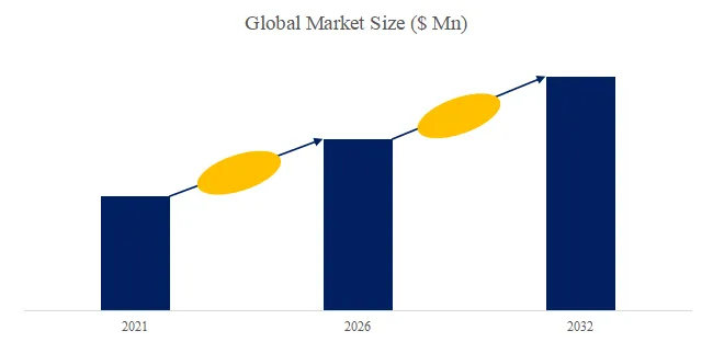
According to the new market research report “Global Thermoplastic Plastic Valve Market Report 2026-2032”, published by QYResearch, the global Thermoplastic Plastic Valve market size is projected to reach USD 2.21 billion by 2032, at a CAGR of 5.1% during the forecast period.
Figure00002. Global Thermoplastic Plastic Valve Market Size (US$ Million), 2021-2032
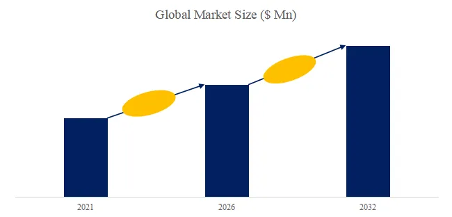
Above data is based on report from QYResearch: Global Thermoplastic Plastic Valve Market Report 2026-2032 (published in 2025). If you need the latest data, plaese contact QYResearch.
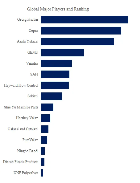
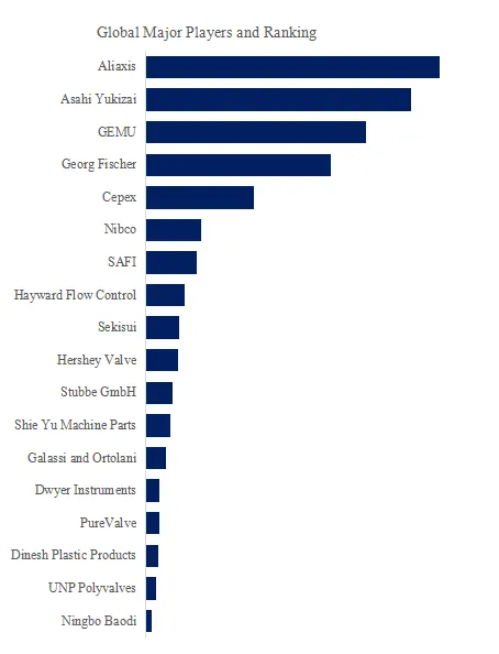
Figure00003. Global Thermoplastic Plastic Valve Top 18 Players Ranking and Market Share (Ranking is based on the revenue of 2025, continually updated)
Above data is based on report from QYResearch: Global Thermoplastic Plastic Valve Market Report 2026-2032 (published in 2025). If you need the latest data, plaese contact QYResearch.
According to QYResearch Top Players Research Center, the global key manufacturers of Thermoplastic Plastic Valve include Aliaxis, Asahi Yukizai, GEMU, Georg Fischer, Cepex, Nibco, SAFI, Hayward Flow Control, Sekisui, Hershey Valve, etc. In 2025, the global top 10 players had a share approximately 60.0% in terms of revenue.
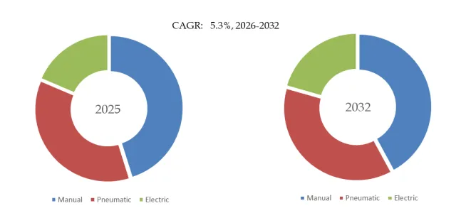
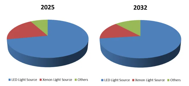
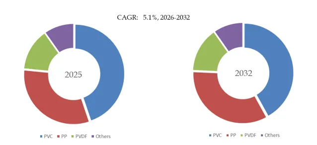
Figure00004. Thermoplastic Plastic Valve, Global Market Size, Split by Product Segment
Based on or includes research from QYResearch: Global Thermoplastic Plastic Valve Market Report 2026-2032.
In terms of product type, currently PVC is the largest segment, hold a share of 44.8%.
In terms of product application, currently Heavy Chemicals is the largest segment, hold a share of 22.4%.
About QYResearch
QYResearch founded in California, USA in 2007.It is a leading global market research and consulting company. With over 17 years’ experience and professional research team in various cities over the world QY Research focuses on management consulting, database and seminar services, IPO consulting (data is widely cited in prospectuses, annual reports and presentations), industry chain research and customized research to help our clients in providing non-linear revenue model and make them successful. We are globally recognized for our expansive portfolio of services, good corporate citizenship, and our strong commitment to sustainability. Up to now, we have cooperated with more than 60,000 clients across five continents. Let’s work closely with you and build a bold and better future.
QYResearch is a world-renowned large-scale consulting company. The industry covers various high-tech industry chain market segments, spanning the semiconductor industry chain (semiconductor equipment and parts, semiconductor materials, ICs, Foundry, packaging and testing, discrete devices, sensors, optoelectronic devices), photovoltaic industry chain (equipment, cells, modules, auxiliary material brackets, inverters, power station terminals), new energy automobile industry chain (batteries and materials, auto parts, batteries, motors, electronic control, automotive semiconductors, etc.), communication industry chain (communication system equipment, terminal equipment, electronic components, RF front-end, optical modules, 4G/5G/6G, broadband, IoT, digital economy, AI), advanced materials industry Chain (metal materials, polymer materials, ceramic materials, nano materials, etc.), machinery manufacturing industry chain (CNC machine tools, construction machinery, electrical machinery, 3C automation, industrial robots, lasers, industrial control, drones), food, beverages and pharmaceuticals, medical equipment, agriculture, etc.
Contact Us:
If you have any queries regarding this report or if you would like further information, please contact us:
QY Research Inc.
Add: 17890 Castleton Street Suite 369 City of Industry CA 91748 United States
EN: https://www.qyresearch.com
Email: global@qyresearch.com
Tel: 001-626-842-1666(US)
JP: https://www.qyresearch.co.jp